14

Consider:

Enter image description here

Attached schematic is from a broken sampling scope that I have in the lab.

During the reverse engineering the module, I noticed that it uses positive feedback around U2. I understand that positive feedback is often used to implement a negative impedance (and thereby extending the bandwidth), but I don't see any advantage in the AC response in an LTspice simulation.

Enter image description here

Green is without 4.2 kΩ and 1.87 kΩ in U2, and Blue is with these positive feedback networks. As shown in the figure, positive feedback reduces both the bandwidth and AC gain.

Edit: parts # for U2~U4 are OP37G.

Emm386
  • 577
  • 2
  • 14
  • 1
    Here are some answers that might help. https://electronics.stackexchange.com/questions/99502/op-amp-positive-negative-feedback-together. https://electronics.stackexchange.com/questions/98354/impedance-to-voltage-range. – mrbean Aug 04 '23 at 05:05
  • 1
    A few more for fun https://electronics.stackexchange.com/questions/466703/positive-and-negative-feedback-in-opamp-in-same-circuit. https://electronics.stackexchange.com/questions/410640/opamp-with-multiple-feedback-loops – mrbean Aug 04 '23 at 05:17
  • Is this in the high frequency signal path or elsewhere? Those “opamps” are probably nothing common. I imagine they would be high-bandwidth parts that may have non-standard pin outs. Please edit the question to include a picture of the part of the module that is shown on the schematic. – Kuba hasn't forgotten Monica Aug 04 '23 at 12:54
  • @Kubahasn'tforgottenMonica I just updated the post. Parts # for U2~U4 are OP37G. – Emm386 Aug 04 '23 at 15:41

2 Answers2

8

The advantage of such a "mixed" feedback is that the resulting total gain can be chosen independently of the feedback factor. This means that the loop gain (and, thus, the phase margin) can also be freely selected, which even allows the use of a non-compensated amplifier. However, it must be noted that of course the negative feedback must prevail over the positive feedback.

Simple example:

  • Positive feedback with R4-R3 (input signal at R3).
  • Negative feedback with R2-R1 (R1 to ground).

Gain: [R4/(R3+R4)] / [R1/(R1+R2)]-[R3/(R3+R4)].

EDIT: This result is correct - even when the forum member periblepsis thinks it would be "simply wrong". Here is the calculation:

V-=VoutR1/(R1+R2) and V+=VoutR3/(R3+R4) + VinR4/(R3+R4).

Setting V+=V- we arrive at the given gain Vout/Vin.

LvW
  • 24,857
  • 2
  • 23
  • 52
  • ah this makes sense. thanks a lot for your response. One question: I used R1=536 Ω, R2=3.34 kΩ, R3=1.87 kΩ, and R4=4.2 kΩ, but cannot get the same gain as what @periblepsis derived. Could you also comment on how you get the gain equation please? – Emm386 Aug 04 '23 at 16:47
  • @Emm386 Gain equation for the first stage only? – LvW Aug 04 '23 at 16:55
  • more specifically, I was curious how you get to the equation at the bottom of your response: Gain: [R4/(R3+R4)] / [R1/(R1+R2)]-[R3/(R3+R4)] – Emm386 Aug 04 '23 at 17:08
  • 1
    @Emm386 I have used, of course, the classical way for finding the gain expression: V+=V- (that means Vdiff=0). For finding V+ you must use superposition because two voltage sources are involved (Vout and Vin). – LvW Aug 04 '23 at 18:40
  • I see what you are doing in the gain calculation. I also missed your assumption. Again, thanks for sharing your knowledge and answering my question! – Emm386 Aug 05 '23 at 17:32
7

Reduction for Analysis

I've reduced the first stage of your schematic to a more behavioral one for analysis:

schematic

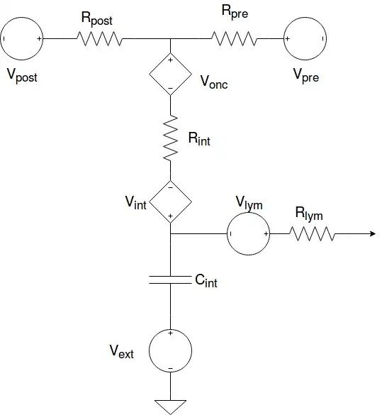
simulate this circuit – Schematic created using CircuitLab

From the above, we know:

$$\begin{align*} V_{_\text{O}}\cdot\frac{1+\frac{R_2}{R_3}}{1+\frac{R_6}{R_7}}&=\frac{\frac{V_{_\text{O}}}{1+\frac{R_4}{R_5}}\,\cdot\,R_1+V_{_\text{I}}\,\cdot\,R_{_\text{TH}}}{R_1+R_{_\text{TH}}+\frac{R_1\,\cdot\,R_{_\text{TH}}}{R_2+R_3}} \end{align*}$$

Loop Gain and Closed Loop Gain

From that, find:

$$\begin{align*} V_{_\text{O}}\cdot\left(1-\frac{\frac{1}{1+\frac{R_4}{R_5}}\,\cdot\,R_1}{R_1+R_{_\text{TH}}+\frac{R_1\,\cdot\,R_{_\text{TH}}}{R_2+R_3}}\cdot\frac{1+\frac{R_6}{R_7}}{1+\frac{R_2}{R_3}}\right)&=V_{_\text{I}}\,\cdot\,\frac{R_{_\text{TH}}}{R_1+R_{_\text{TH}}+\frac{R_1\,\cdot\,R_{_\text{TH}}}{R_2+R_3}}\cdot\frac{1+\frac{R_6}{R_7}}{1+\frac{R_2}{R_3}} \end{align*}$$

That's in the form of \$V_{_\text{O}}\cdot\left(1-B\cdot A\right)=V_{_\text{I}}\cdot A\$ with \$A=\frac{R_{_\text{TH}}}{R_1+R_{_\text{TH}}+\frac{R_1\,\cdot\,R_{_\text{TH}}}{R_2+R_3}}\cdot\frac{1+\frac{R_6}{R_7}}{1+\frac{R_2}{R_3}}\approx 0.877\$ and therefore \$B=\frac{R_1}{R_{_\text{TH}}}\cdot \frac{1}{1+\frac{R_4}{R_5}}\approx 0.419\$.

It's also in the positive/regenerative feedback form, as you already identified. So \$B\$ is positive feedback. The loop gain is \$A\cdot B\approx 0.368\$ and since this is less than 1 the system converges on the overall closed loop gain of \$\frac{V_{_\text{O}}}{V_{_\text{I}}}=\frac{A}{1-B\,\cdot\, A} \approx 1.39\$.

So, expanding \$\frac{A}{1-B\,\cdot\, A}\$, the final closed loop gain equation is:

$$A_v=\frac{1+\frac{R_6}{R_7}}{\frac{R_1}{R_3}+\left(1+\frac{R_2}{R_3}\right)\,\cdot\,\left(1+\frac{R_1}{R_4}+\frac{R_1}{R_5}\right)-\frac{R_1}{R_4}\,\cdot\,\left(1+\frac{R_6}{R_7}\right)}$$

Let's test both:

def par(a,b): return a*b/(a+b)         # a and b taken in parallel
a = par(r4,r5)/(r1+par(r4,r5)+r1*par(r4,r5)/(r2+r3))*(1+r6/r7)/(1+r2/r3)
b = r1/par(r4,r5)/(1+r4/r5)
(a/(1-b*a)).subs( { r1:1.76e3, r2:3.64e3, r3:1.76e3, r4:4.2e3
                  , r5:1.87e3, r6:3.34e3, r7:536 } )
1.38762233798678                       # computed using A/(1-B*A)
(r6/r7 + 1) / (r1/r3 + (r2/r3 + 1)*(1 + r1/r5 + r1/r4) - r1/r4*(r6/r7 + 1)).subs(
    { r1:1.76e3, r2:3.64e3, r3:1.76e3, r4:4.2e3
    , r5:1.87e3, r6:3.34e3, r7:536 } )
1.38762233798678                       # computed using expanded version

Note that they are both equivalent to each other. Just two different ways of saying the same thing. So the voltage gain is \$20\cdot\log_{10}\left(1.38762233798678\right)\approx 2.84542565\:\text{dB}\$

I've added a test using LTspice (performed a day after the answer was written):

enter image description here

Seems that LTspice agrees.

Input Impedance

To get this, I simply derived it by first taking the voltage difference across \$R_1\$ and dividing that by \$R_1\$ to get the current in \$R_1\$. This current was then divided into the input voltage in order to work out the impedance. It's straight-forward.

The input impedance thus seen by the source will be:

$$R_{_\text{I}}=R_1\cdot\frac{1}{1-\frac{V_{_\text{O}}}{V_{_\text{I}}}\cdot\frac{1+\frac{R_2}{R_3}}{1+\frac{R_6}{R_7}}}\approx 2.432\times R_1\approx 4.28\:\text{k}\Omega $$

Schematic Notes

The following shows my notations for the schematic used to derive the above:

enter image description here

periblepsis
  • 3,766
  • 1
  • 1
  • 10
  • Thanks a lot for the detailed comment. can you double check if R4 and R5 in figure are typo? I cannot find these components from your figure. – Emm386 Aug 04 '23 at 15:45
  • @Emm386 Sure. I'll add my notes at the end of of my answer. – periblepsis Aug 04 '23 at 15:51
  • 1
    @Emm386 Let me know if there are further questions. – periblepsis Aug 04 '23 at 15:59
  • thanks for the update. I have another quick question: could you also elaborate on how you come up with equation for the input impedance? – Emm386 Aug 04 '23 at 17:50
  • 1
    I really want to accept this as an answer for my question, but I think response from LvW is more close to what I was looking for: the reasoning of positive feedback. But again, I really appreciate you for providing all the analysis and detailed explanation. I would greatly appreciate if you can elaborate on the input impedance calculation too!! – Emm386 Aug 04 '23 at 20:17
  • 1
    @Emm386 That's very nice of you to say. But please don't worry. Just saying what you said is all I care about. So thanks! Very much appreciate the thought. And be happy! (I don't do any of this for points.) Just keep in mind that LvW's gain equation is ... not correct. Given your resistor values it comes out with 1.867. Which is much too high. Check it out. – periblepsis Aug 05 '23 at 01:08
  • Thanks a lot for understanding and extra comments. Regarding the input impedance calculation, did you use Blackman's equation? or is this a different way of approaching the input impedance calculation? – Emm386 Aug 05 '23 at 03:18
  • @Emm386 I simply derived it by taking the voltage difference across R1, divided by R1, to get the current in R1. This current was then divided into the input voltage to work out the impedance. It's straight-forward. No fancy named method. Just *plain applied logic*. (I've added the gain for the system to my answer.) – periblepsis Aug 05 '23 at 03:51
  • 1
    ah I see. yeah I was being stupid. As what you said exactly, this was a straight-forward computation. again, thanks a lot for detailed comments and everything! I learned a lot from you. – Emm386 Aug 05 '23 at 04:54
  • 2
    @Emm386 I've added a run from LTspice to the answer and updated a few details. I am quite flummoxed by LvW's gain expression. It's simply wrong. – periblepsis Aug 05 '23 at 05:57
  • 1
    I also couldn't replicate the equation from my side. But I generally agree with his intuition about freedom over stability. – Emm386 Aug 05 '23 at 06:33
  • @periblepsis Just to say "simply wrong" is not enough. It would be very helpful if you could give the gain expression which you would consider as correct. Perhaps you did not notice that I was speaking of an amplifier with 4 resistors only (as mentioned in my contribution)? – LvW Aug 05 '23 at 08:24
  • 1
    @LvW You can see such a gain equation in my writing. It's already there and verified. I assumed you were directing your gain equation to the questioner's schematic. That assumption may then be my own error, not yours. My apologies for just skimming and projecting. Thanks for the reminder that I should read more closely before writing like that. – periblepsis Aug 05 '23 at 09:13
  • OK - these things can happen from time to time. – LvW Aug 05 '23 at 18:52