9

I have a small hobby project in which I want to include the Kingston EMMC04G-M657 eMMC chip. This chip comes in BGA packaging with 0.5mm pitch between balls. I want my board to be cheap, so I'm laying it out for a 4-layer JLBPCB PCB using their standard rigid board design rules. These rules specify:

  • Min trace width: 0.09mm
  • Min trace spacing: 0.09mm
  • Min Via hole size/diameter: 0.15mm / 0.25mm

I've put these rules into KiCAD and it seems to me that there are a few pins that I can neither escape from the BGA with a trace nor disappear with a via:

enter image description here

KiCAD will actually let me place a via right on top of the pad, but I imagine that is a really bad idea, right?

enter image description here

If I want to use this chip, will I have to use some special manufacturing process? Or am I misunderstanding something here? I'm sure as you can tell from my questions I am a real noob, so don't assume too much prior knowledge.

JYelton
  • 32,302
  • 33
  • 134
  • 249
Mr Squid
  • 201
  • 4
  • A via with a tiny hole is probably OK. What size via holes do the rules allow? – Andy aka Aug 01 '23 at 20:09
  • 6
    Via in pad is typically done for BGA parts with tight pitches. The fabricator needs to drill the via, plate the hole, fill the hole (so solder doesn't run down the drain), planarize the pads (make them flat enough for soldering), and finally plate. The fill and planarize are extra steps which add cost. – C. Dunn Aug 01 '23 at 20:17
  • 1
    Why are your pads not aligned properly? 3B, 3C and 3D do not seem to be aligned along the Y-axis. – Durmus Aug 02 '23 at 15:35
  • 1
    If this is a small hobby project, you can buy eMMC modules attached to a small connectorized board. In fact, many large production projects do this, so the eMMC can be programmed separately, they can swap the main board in the field while preserving device information, they can sell multiple models with different storage, etc. – user71659 Aug 02 '23 at 16:44

2 Answers2

16

For this sort of routing, you will need to do a 'via-in-pad' technology. Essentially, just place the via centered on the pad.

JLCPCB offers this on their 6-layer process standard and on 4-layer board for an extra charge. They call it 'POFV' or 'plating over filled via'.

Seth
  • 4,482
  • 15
  • 23
  • 2
    Do I need to do something special in my EDA software to indicate that I'm placing one of these special vias? – Mr Squid Aug 01 '23 at 20:34
  • 1
    @MrSquid for JLC, nothing special required to indicate plated via - they will do all vias as POFV below a certain size (<=0.5mm drill IIRC) as standard on the 6 Layer stackups. – Tom Carpenter Aug 02 '23 at 00:31
  • 2
    @MrSquid note that the [JLC Guidelines](https://jlcpcb.com/help/article/243-BGA-Design-Guidelines---PCB-Layout-Recommendations-for-BGA-packages) about POFV and BGAs says "The vias are filled with either conductive or non-conductive epoxy. Minimum drill is 0.2 mm, so use 0.3 mm pads.". That would leave 0.2mm spacing between pads which is acceptable. – Tom Carpenter Aug 02 '23 at 00:36
9

As @Seth answer indicates, plated via-in-pad is the technology used to acheive this. For really dense chips this is frequently in combination with laser drilled blind micro-vias, though that is beyond most PCB pooling companies.

In your case as there are not many balls to pin out a simple plated via in pad to get to other layers should make things possible. As mentioned JLC support this POFV option if requested on 4L (or by standard on >6L).

Indeed looking at the pinout for the chip, most of the balls are "NC" which the datasheet indicates are not electrically connected to anything. This means you can route e.g. power traces through those other balls to help escape route things. When doing this, leave the pads on the PCB so the balls get connected otherwise assembly may fail, but you can assign the NC pads to whatever purpose you wish to help you escape route.

NC indicated as not electrically connected


Regarding JLC, make sure you read their guidelines if you plan to do via in pad. Specifically they say for BGA via-in-pad with POFV:

The vias are filled with either conductive or non-conductive epoxy. Minimum drill is 0.2 mm, so use >=0.3 mm pads.

Because of this restriction, the pad size for your BGA must be set to at least 0.3mm, with a 0.2mm drill to use the via-in-pad option here. This is quite large for a 0.5mm pitch BGA, but not insurmountable.


When choosing the size of the BGA pad, you should consult with either the manufacturers recommended sizes, or if not specified, make use of tables listing common pitch/ball sizes to determine the specific required solder mask openning and pad sizes.

Your device datasheet indicates a pitch of 0.5mm and a ball diameter of nominally 0.3mm. Based on the tables here, you will have to go for the "Solder Mask Defined (SMD) Pad" approach. For this pitch/ball diameter, the table calls out:

Pad Size for SMD pads table

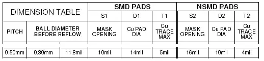
Note that for the NSMD option, the copper pad size required 0.26mm (10 thou) which is too small for the JLC via, and therefore cannot be used.

Instead, for the SMD option, the table gives a copper pad size of 0.35mm (14 thou). This is larger than the size of the via annulus so should work well. Then make the aperture in the solder mask of 0.26mm (10 thou).

Tom Carpenter
  • 63,168
  • 3
  • 139
  • 196