2

I'm working with audio codecs, and I have to put a lot of them (32) on a PCB.

The fact that I have to connect so many ICs makes the board pretty big with very long tracks. I've read a lot about how to handle the design properly to avoid crosstalk and interferences, but I'm still struggling to find a definitive answer.

So, I want to connect 32 MAX98357 codecs in TDM (Time-division multiplexing) mode. This codec also acts as a small amplifier. I control them with a FPGA Zynq (Zybo Z7). The FPGA controls only 3 digital signals per codec (Bit Clock, Word Select, and Data). They all share the same two clocks (Bit Clock and Word Select), which are around 100MHz. Each bank of 8 codecs shares the same Data line (the codecs know his slot thanks to a resistor).

To achieve this, I basically replicated the layout from the Adafruit breakout board 32 times. Additionally, I added a clock buffer (551SDCGI) for the 3 digital signals and put 8 codecs per output. Below is one bank of 8 codecs and their connections: (I highlighted a clock line) enter image description here
The signal comes from the right connector, goes through the clock buffer, and is then distributed to all of the codecs.

The big capacitor in front of each of them is to stabilize the power supply because they are all amplifiers too, but I'm not entirely sure about this part.

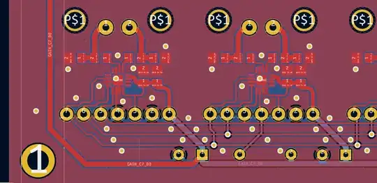
Due to PCB constraints, I can only use a 2-layer PCB. I poured GND on each side and added stitching vias as shown below:

enter image description here enter image description here

The 3 parallel lines are my 3 digital signals (clock and data).

Now, my question is about the stitching vias. Is my implementation okay, or is it overkill?

From what I read, since the maximum frequency is 100MHz, even if I take 1/20 of the wavelength as the distance between vias, it might be overkill (3m/20=15cm).

On the other hand, I also read that if I just pour GND between lines without stitching it, I will have an antenna effect.

So, what should I do? Is it enough to have GND on the bottom layers without top and stitching vias?

Do I have to calculate the wavelength with 100MHz, or is it different because it's a square digital signal?

I know this question is pretty frequent, but I never find this kind of strange implementation (not to high frequency but very long track) I hope I give enough information for you to help me...
JYelton
  • 32,302
  • 33
  • 134
  • 249
Max_Pof
  • 21
  • 2
  • F_max on the MAX98357 in TDM mode is 25MHz. Where does 100MHz come from? – user1937198 Aug 01 '23 at 16:11
  • Maybe the edge rate??? – SteveSh Aug 01 '23 at 16:23
  • What purpose do you thing the stitching vias serve? What problem, or potential problem do you think they will prevent? – SteveSh Aug 01 '23 at 16:25
  • And the only reason I can see for the stitching vias is to try and compensate for the fact that your ground planes are all chopped up into little bitty sections. – SteveSh Aug 01 '23 at 16:28
  • I have a similar project with another codec that uses a 98.304 MHz clock. That's why I rounded it to 100MHz. However, I didn't expect that the difference between 25MHz and 100MHz would matter so much. Should I consider the clock rate or the edge rate? – Max_Pof Aug 01 '23 at 19:18
  • "What purpose do you thing the stitching vias serve" I would say avoiding long, narrow ground planes between the lines as they may behave like antennas and introduce additional noise..? No? – Max_Pof Aug 01 '23 at 19:21

2 Answers2

2

Your approach is probably good. Ideally you separate signal traces so that you reduce or eliminate crosstalk. Putting copper between the traces can negatively affect this, because it aids in crosstalk... unless you properly ground and stitch it with sufficient vias.

In some designs, such as those containing high-speed data or RF signals >1GHz, the ground pour can be helpful as shielding, but then you should be thinking of transmission lines (microstrip/stripline, etc.) with via fencing.

Eric Bogatin, in an Altium Academy video titled "You Must Unlearn What You Have Learned", demonstrates how copper pours (at this time index) can adversely affect boards. To summarize:

  • If your traces are >3W apart (this is a "rule of thumb" where W is the trace width), the crosstalk should be minimal. (Good)

  • If you add copper fill but leave it floating, it can make the crosstalk worse. (Worst)

  • If you via-stitch to ground sufficiently on the pour, it can decrease crosstalk more than having no copper at all. (Best, but does not have a great risk/reward ratio.)

The crosstalk amount is highly dependent on the amplitude and rise time (Δv/Δt) of the signal and the length of the trace.

JYelton
  • 32,302
  • 33
  • 134
  • 249
  • Whoa! Thank you very much, this is a very interesting video! And I think I have my answer now, I will definitely remove the ground pour and the vias! – Max_Pof Aug 01 '23 at 19:40
  • Just to be sure, when [some guidelines](https://resources.pcb.cadence.com/blog/2021-how-to-reduce-stray-capacitance-in-electronic-circuits) recommend to shield the conductor to reduce stray capacitance, it's the same thing: it's true only if it's correctly done? Or are we talking about something different? – Max_Pof Aug 01 '23 at 20:18
  • Separation depends on substrate height (dielectric height above nearest ground plane) as well; preferably be greater than 3*max(W, h). I would even go farther and strengthen the "some designs" range: PCB foil is an effective shield at even just a few MHz; and transmission line concepts being not just helpful, but *critical* at >100MHz. – Tim Williams Aug 01 '23 at 21:44
  • @Max_Pof Stray (or parasitic) capacitance is the capacitance between two traces or planes of different potential, where the space in between, be it FR4 or air, forms the dielectric. Placing copper ground pours with plenty of via stitching can reduce stray capacitance as per your link. You can [calculate](https://electronics.stackexchange.com/q/56574/2028) it and determine if it affects your application, though it's not usually a problem until you are designing transmission lines with controlled impedance and need to factor it in. – JYelton Aug 01 '23 at 22:42
1

Now, my question is about the stitching vias. Is my implementation okay, or is it overkill?

It's overkill unless you are working in the sub uV level or fast signals (50MHz+). Since you have signals that are 100MHz it's probably a good idea.

That via adds ~1nH of inductance between layers so the return currents will be able to go between layers on the ground through the via. The return currents will follow the lowest impedance pathway, if it's not under the trace then it will slow the signal down.

Another thing that you need to do is really minimize capacitance and inductance so you can get fast rise times.

Voltage Spike
  • 75,799
  • 36
  • 80
  • 208