I found one valuable Utmel blog which explains the three things:
The internal chip can be erased by irradiating ultraviolet rays through the hole. The EPROM eraser is needed to complete the chip erasing operation.
PROM is a programmable device. The mainstream product adopts a double-layer gate (two-layer poly) structure, including EPROM and EEPROM.
And EEPROM and EPROM internal structure seems to be same because they both use the double-layer gate:
eliminate the electron in EEPROM
I also found another Naver blog which compares EPROM and EEPROM although I don't master the Korean language:


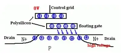
From the 3rd figure, the EPROM has no circuit to induce electrons while the EEPROM has by using WL,BL to control the electron induction in the double-layer gate. This shows how NOR flash (one type of the EEPROM) works.
Q1: EPROM and EEPROM are only different that they use different erasing technology but the internal structure are same.
Are the statements right?
P.S. Answer to the old 2nd question in the history: reading EEPROM by using one "intermediate voltage" is similar to how DRAM is read