Thanks to your advice on StackExchange, I'm in the final stage of developing my first LM5143A-Q1-based (link to datasheet) buck converter! It may be a bit rushed as I need to prepare this for a high school project and I'm still learning, but positive criticism is highly welcomed! The problem now is, routing. I would appreciate it a lot if you could take a look at it and tell me if there are any issues. What could be improved?
EDIT: High Quality (.SVG) images are available to download at this link. I wanted to place them in this post but the website doesn't accept this format.
This is the schematic, all done in Kicad:

This is the layout: Top Layer, all components mounted here

GND Layer

VIN Layer

The Bottom Layer, yes, big trace

There are a couple of quick questions I have about the visuals:
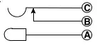
- Take this via for example. Does the black area between it and the PWR (VIN) plane mean it's isolated from the plane? Else it would be shorted!

2.Take this via for example. If the standard trace goes into the filled zone, does that mean it's making contact and they're connected? Since it should

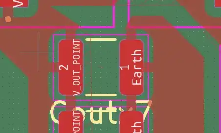
If the via is itself isolated, is there any reason to make another isolation copper island like in the photo below?
Is there any reason to use these "thermal reliefs" over standard tracks? (I did it since I heard they're good)


The layout was highly inspired by Brian's 4 layer board. (except from his perfect copper islands) From him and all the resources I searched, I understood a couple of basic design rules:
- Ground Plane always underneath IC
- Keep traces as short as possible (well, except for that huge L1-L2 connection on the back... How big of a problem will it be?)
- Use filled zones instead of traces when possible
- Keep all high freq parts on the same side
Thank you in advance for any advice! It's the first time I'm doing something like this and I loved learning it!