0

I have a requirement to generate a 4 sec pulse when a switch is closed and another pulse when the switch is open with minimal (<10uA) to zero power consumption when the pulses are not being generated.

Vin is between 6.5 & 3.3v (due to battery life).
Vout Pulse voltage should match Vin.

We have the below circuit currently however, Vout doesn't match Vin.

Additionally I may switch the physical switch to an open drain component which would pull IN and can either be floating or pulled high as required.

Can anyone suggest a lower power & better circuit please? I'm open to any suggestions such as flip-flops or 555 timers so long as it meets the above requirements.

Many thanks as always.

schematic

simulate this circuit – Schematic created using CircuitLab

  • What happens if the button is released before 4 seconds have occurred? How do you plan to deal with contact bounce and, how much delay can you tolerate when using a debounce circuit? – Andy aka Jul 19 '23 at 11:53
  • You definitely don't want to use a 555. Quiescent current is typically in the 2-3 mA range and can be as much as 15 mA. – WhatRoughBeast Jul 19 '23 at 15:01
  • Debounce would be helpful @Andyaka as this will be used to initialise an MCU although not essential, I think about 1.5-2sec is ok – Planestoner Jul 19 '23 at 23:56

2 Answers2

1

You're very close. The simulation in CircuitLab does not account for the schmitt trigger inputs of the CD4093, and so you won't see the true duration of output pulses. Also, the gates are not simulated with any particular supply voltage, so their outputs are "digital high or low", showing up as 1 or 0 on the graphs. If you want to simulate this properly, use LTSpice, or something similarly high-tier.

The circuit I suggest is as follows:
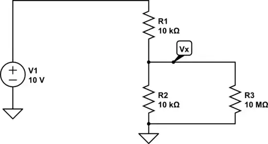
schematic

simulate this circuit – Schematic created using CircuitLab

This employs a single-throw "open/closed" switch, instead of your double-throw relay switch, since that's how you described it in the question. R3, R4 and C3 debounce the switch contacts, and I also added gate G3 to clean up and buffer the switch signal. The schmitt trigger inputs of the CD4093 will help enormously with immunity to noise and interference. You probably couldn't get away with such large values for R3 and R4 if using regular gates, so don't use regular gates.

The only real long-term current drain from the power supply is due to R3 and R4. When the switch is closed, these resistors cause about 10μA to flow from the supply. You could increase those resistances to decrease current, but I feel that they are already very high. I don't see any simple alternative, if you use a single-throw switch.

G3 also adds symmetry to charging and discharging of C1 and C2. Both paths now have similar source impedance driving them (and other characteristics), to keep the two pulses of similar duration.

When using schmitt trigger input gates, the switching thresholds will be near \$\frac{1}{3}\$ and \$\frac{2}{3}\$ of the supply, which means that the duration of the pulses will be very close to time constants \$R_1C_1\$ and \$C_2R_2\$. The values I use of 10μF and 470kΩ should yield pulse durations close to 4 or 5s.
Simon Fitch
  • 27,759
  • 2
  • 16
  • 87
  • Capacitor selection, especially C3 is going to important. – WhatRoughBeast Jul 19 '23 at 15:04
  • @simon-fitch This really helps thank you, especially to include the debounce and a SPST switch to ground. This gives me a lot of options. When you say _dont_ use regular gates, can you provide any recommendations? Most chips have either VDD of 6V or 18V and with the 6.5V battery supply I'd imagine that removes a good chunk of options. – Planestoner Jul 19 '23 at 23:48
  • @WhatRoughBeast, yes you're right. Are you referring to capacitor type or value? – Planestoner Jul 19 '23 at 23:51
  • Also @simon-fitch if I was to read the switch position with a GPIO would you place that before or after R4? – Planestoner Jul 19 '23 at 23:56
  • @Planestoner For supplies over 6V you're pretty much stuck with 4000 series CMOS ICs. The 4093 is the only NAND I'm aware of. It's a great choice though, since it has very low quiescent supply current. – Simon Fitch Jul 19 '23 at 23:58
  • @Planestoner I would read switch state from the output of G3. That a nice clean signal for the MCU, but don't forget that at 0V/+6.5V it is incompatible with the MCU. You'd have to scale it somehow, but that would probably require extra quiescent current. – Simon Fitch Jul 20 '23 at 00:02
  • @Planestoner - Especially type. Dielectric types have wildly different leakage characteristics. – WhatRoughBeast Jul 22 '23 at 02:55
0

How about basic monostable circuit. Since it is latched there is no problem with contact bouncing. It drains nothing when inactive (both BJT are off). You have to add a similar RC trigger to PNP base to react on both edges.

schematic

simulate this circuit – Schematic created using CircuitLab