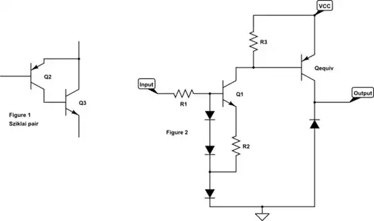
The schematic below describes the structure of a single channel from the 8-Channel Darlington Current Driver TD62783A.
 Image source: 8-Channel Darlington Current Driver TD62783A
I understand most of the circuit's workings but I fail to understand why the PNP transistor exists.
I was thinking that it exists to push current from its base to the collector of the transistor Q1 and that the whole PNP and Darlington section of the circuit acts as an active load for the constant current source centered on Q1. But the presence of the high-value resistor R3 confuses me as I don't see any clear purpose for its presence, perhaps to help with biasing the PNP?
How would I go about analyzing the functioning of the PNP transistor and can I determine the values of the currents passing through it?
EDIT:
As it stands, my current understanding of the circuit is:
The purpose of the circuit is to ensure as big as possible of an output current, not a constant current.
The constant current source is used to "absorb" the variations in supply voltage.
The Darlington pair formed by Q3 and Q4 must be driven high-side, hence the use of Q2.
R3, R4 and R5 are high-valued resistors that discharge the base-emitter capacitance and insure a quick turn-off.
The gain of the "high-current triple" formed by Q2, Q3 and Q4 is gigantic and as such any leakage current from Q1 (EM interference, stored charge or otherwise) might turn on the LEDs unwantedly. We aim to use R3 to solve this issue.
It's still a bit unclear to me if Q2 is supposed to be saturated (and act as a switch) or in the active region (and boost the current gain of the Darlington pair).
SECOND EDIT:
I've come across this answer on stack exchange and I now can better understand sphero's and AnalogKid's answers.
simulate this circuit – Schematic created using CircuitLab
Q2 is indeed an inverted high-side switch. When we turn on Q1, VB2 will be VCC - 0.7V and the PNP inverter will have it's output high. When Q1 is off R3 pulls the base of Q2 to VCC and because VB2 > VCC - 0.7V the inverter outputs a very low voltage.
So in my mind, R3 now has two roles:
- to speed-up the turnoff
- to decrease the voltage at the base of Q2 so that Q2 isn't always off
I also think that the number of LEDs connected to the output is also important, if we have too few connected, Q2 will be in the active region because VEC2 will be much larger than VEB2.
When no load is connected I think we rely on the diode nearest to R5 to keep VOUT high and keep Q2 saturated. During normal operations the diode will only divert an extremely small reverse leakage current from the main flow.
