I refer to the AD711 datasheet.
This behaviour can be expected from any op-amp with finite bandwidth. In your case, the problem is due to a few things:
High gain (100). The op-amp itself introduces phase shift between input and output. If the output were unloaded, gain-bandwidth product of the AD711 is 4MHz. With gain at 100, this places a pole at \$\frac{4MHz}{100}=40kHz\$, where phase shift is at 45°, but onset of phase shift occurs well below this frequency. As phase shift diverges from zero (or, strictly speaking, 180°, as this is an inverting amplifier), the output changes more and more out of phase with the input, and the usual equalisation of inverting and non-inverting input potentials is less and less perfect.
Heavy output loading. R10, the 1kΩ feedback resistor around U2, is making it hard for the op-amp output to keep up with the input. Unloaded, the AD711 has a gain-bandwidth product of 4MHz, but the datasheet also specifies that at full power output, this can drop to 200kHz. You are getting close to full power with such a load as R10.
I would also hazard a guess that the slightly non-sinusoidal trace of the virtual ground suggests that slew rate is also a factor here. With such a heavy load, I imagine that the slew rate has also dropped significantly from the 20V/μs specification, resulting in those somewhat straight-ish portions of that trace.
I'll redraw the section in question. Of interest to you here is the relationship between the signals \$V_{OUT}\$, \$V_{CURRENT}\$ (blue) and \$V_{VIRTUAL}\$ (orange), in the following bode plots of frequency response to \$V_{OUT}\$:
simulate this circuit – Schematic created using CircuitLab
Gain:
Phase:
The gain plot shows a clear roll-off of 20dB/decade at the breakpoint of 40kHz. I've set a green marker at the 10kHz point, and in the phase plot it's clear that phase shift has already begun at that frequency.
The most important trace here is the orange gain plot for \$V_{VIRTUAL}\$. If it were always true that an op-amp with negative feedback acts to equalise its two inputs, then that would be a flat line, of near-zero gain, right across the spectrum.
Obviously here that isn't the case, and from this graph you see that at 10kHz, the amplitude of \$V_{VIRTUAL}\$ is about 10dB down (one third) of \$V_{OUT}\$!
Update
Using U2 as a transimpedance amplifier to provide a virtual ground, and an output proportional to load current seems like a good idea, but it requires U2 to be able to source and sink all current through he load too. That means you would have to bolster the current capability of U2 with a buffer like the one that you used for U1.
Such an arrangement would permit you to measure current without the need for a sense resistor R1, since all load current flows via R10 anyway, with or without R1. R1 only serves to develop some voltage that should otherwise appear across the load, and introduce an error to the measurement.
To increase bandwidth, and maintain a virtual ground at high frequency, feedback resistor R10 should be similar to the load's impedance. Certainly not more than a factor of four greater, to keep loop bandwidth at 1MHz or above:
simulate this circuit
Update 2
Failure to achieve a virtual ground even at DC is clearly a problem with the op-amp being unable to produce sufficient output potential. It's probably a combination of the op-amp being asked for too much current, and R4 and R7 (10Ω) and R10 (4Ω) reducing loop gain considerably.
Driving 1Ω is difficult! You'll need a much better buffer stage to achieve 100mA through R11. Try this:
simulate this circuit
It's a "diamond buffer". This particular incarnation should permit you to drive a load of 1Ω with up to 1A or so. Q1 and Q4 (and their periphery) are 20mA current sources, used instead of your resistors R1 and R22 (5kΩ), which are huge problems in your own design, since they starve the transistors of the base current they need. They can't be reduced without overloading the op-amp, so you have to take a different approach.
I should also point out that with supplies of ±15V, all the transistors here are stressed, the power dissipated everywhere is much greater than necessary. If you could reduce the supplies to ±10V (or even further, without compromising the op-amp, of course), this will make a big difference. You'll still need to use power transistors for Q5 and Q6, as they dissipate over 1W.
Update 3
There's another approach which requires only one current buffer stage:
simulate this circuit
U1 is responsible for maintaining \$V_B = V_{IN}\$, by using negative feedback. It produces whatever potential \$V_A\$ is necessary to achieve that equality, even accounting for \$R_S\$ in its output current path.
All load current current \$I_L\$ must pass via \$R_S\$ anyway, so we have a voltage across \$R_S\$ representing load current. The second op-amp U2 is configured as a unity gain difference amplifier, producing \$V_{CURRENT} = V_A - V_B\$, which is the voltage across \$R_S\$, and therefore a measure of load current.

 The load is 10 Ω resistance.
  The voltage of the virtual ground (inverting input -- blue line) is much higher than I like (almost half the driving voltage). What might be an explanation for this? Is there a way to fix this, to make it closer to ground? I suspect the culprit is the high current ~1 mA that the op amp has to sink. If this is the case, how should we bypass the op amp and drain this current after it passes through the feedback loop? If I change to bigger load 1 kΩ, the current is smaller ~10 uA, and the virtual ground is closer to the ground.
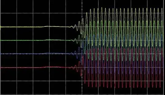
 I got time scan of virtual ground:
 Bode plot:
 The virtual ground's amplitude of oscillation is much less compared to the non-boosted current sensor, but it has an offset. I have trouble understanding where that offset comes from and how to fix it.
