1

We are an association of French students learning electronics. I'm actually making a circuit to make a quartz clock, I'm looking over the schematic that I found on the net, but I really don't know why these Components were chosen and why these values.

The components that I really don't understand are:

  • C101 (why this value ?), D110, R101, R102 , R103, D108, C105, R105

and for the crystal:

  • C103, C104 and R104.

Clock 004

Power and oscillator

Source: Horloge 004

Greenonline
  • 2,064
  • 7
  • 23
  • 38
Anthox
  • 81
  • 4
  • 3
    The reason why these exact component values is unknown unless the text on website explains it. Most values are just generic and likely pulled out of hat as they will work as long as they are in the right ballpark, i.e. not 10x too small or 10x too large. Some values may be calculated, but the values used for crystal do not look very sensible, unless the crystal or circuit demands such values. But we don't know what crystal it is. I am afraid there may not be an answer why exactly each component has that specific value. – Justme Jun 27 '23 at 15:01
  • A notable feature of this clock is that as well as mains-derived frequency, it has battery backup and 32.768 kHz crystal circuit -- which is very common in French clocks. English clocks more usually just fail if their power goes, possibly with a latch so it knows it hasn't been set since power up. (This typically is used to inhibit counting, or sometimes flash the whole clock at 1 Hz.) And it appears to switch off the LEDs with Q101 if mains is off, presumably to maintain time without using up battery. – jonathanjo Jun 27 '23 at 15:09
  • As @Justme suggests, C103, C104 appear to be in the 10X-too-large ballpark. C101 is determined by current needed. The CMOS logic chips require very little current, but those LED display numerals require much more, and those giant LED digits shown in the article require even more current. Seems illogical to use LED digit display for a clock that is intended to run when AC power is unavailable. – glen_geek Jun 27 '23 at 15:16
  • 1
    @glen_geek ... the LEDs are grounded to `0V_Aff` ("display ground") turned off by Q101 when there's no AC. – jonathanjo Jun 27 '23 at 15:23
  • Ok so the quartz has to have a datasheet to look for the correct values to input ? Because i've just read an article from texas instruments (https://www.ti.com/lit/an/szza043/szza043.pdf) explaining where to find values. The problem of the circuit is that i want to understand everything to explain to other students. Thanks for your explanations for the crystal and the C101. I think i'm going to make a Pierce Oscillator with inverter so i can more understand how it works. One thing also that i don't understand it why there are so many diodes like D111 or D110 ? because the voltage is already + – Anthox Jun 27 '23 at 15:38
  • D110 and D111 form an OR gate, so either the crystal circuit or the line-derived circuit can provide the 1 Hz clock. Most of the other diodes are also used to form OR gates. R105 and many other resistors are pull-down resistors that pull the outputs of the diode OR gates Low when a diode is not pulling the output High. – Peter Bennett Jun 27 '23 at 15:49
  • D111 and D110 is OR gate. So both Clk sources (Quartz or 100Hz from mains) can create 1Hz signal. – Michal Podmanický Jun 27 '23 at 15:50
  • D110, D111 and R105 make a [wired-or](https://en.wikipedia.org/wiki/Diode_logic#Active-high_OR_logic_gate) gate. Notice that `PS_on` drives the master reset of U104 to stop the crystal circuit counting. – jonathanjo Jun 27 '23 at 15:51
  • 1
    @Justme I wonder if someone read "220" off the component ... which would be 22 pF! –  Jun 27 '23 at 17:26
  • "I think i'm going to make a Pierce Oscillator with inverter" - that's exactly what this circuit is making with the inverter inside the CD4060 between RS and RTC. But it then uses a Schmitt trigger that cleans up the waveform to make it nice and square as the oscillator produces slow rise and fall times which are not good for CMOS inputs. – Finbarr Jun 27 '23 at 17:28
  • In the moment U104 is stopped because the AC supply recovers, the output of U105:A may be just high and stay there and the clock will stop, whatever U103 delivers. So this is a 50% chance stop clock. – Jens Jun 27 '23 at 18:04

2 Answers2

1

The crystal oscillator employs an inverter gate in the role of an analogue inverting amplifier, not a digital one. The gate on its own has a very non-linear input-to-output relationship, and inconveniently high gain. R104 provides negative feedback, which reduces gain, and improves linearity (and bandwidth), in the same way feedback resistance with an op-amp does. It just converts what was a digital gate into a better-behaved analogue amplifier.

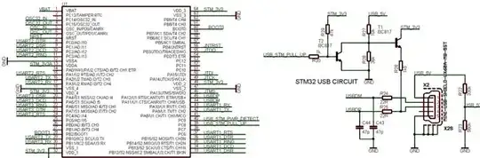
The two capacitors C103 and C104 ensure that the crystal oscillates at its rated frequency. How they do this, and how you calculate their value, is a big topic, but you can read about it here. The crystal's documentation specifies a "load capacitance" \$C_L\$, and this value will decide the values of C103 and C104. In this schematic, the value of 220pF seems rather large.


C101 is the power supply filter capacitor. They way the schematic is drawn make it difficult to see its role, so I'll redraw a simplified version here:

schematic

simulate this circuit – Schematic created using CircuitLab

The diamond-shaped bridge rectifier represents the diode bridge formed by D101, D102, D103 and D104. If C101 were absent, the potential \$V_S\$ at the output of the rectifier (node S) would look like this:

enter image description here

This is just the full-wave rectified AC signal, with a frequency of 100Hz, which is clearly not good enough to power a DC circuit, so C101 is included to smooth it out, to a persistently high DC potential. With \$C_{101}=1000\mu F\$, and a load current \$I\approx 100mA\$, \$V_S\$ looks like this:

enter image description here

Capacitor C101 gets "topped up" with every peak of the rectified source, but slowly discharges between peaks, due to current being drawn by the load. The result is potential "ripple" at S. A larger value for C101 will produce less ripple, since it will discharge more slowly between peaks. A smaller value will cause it to discharge more quickly, causing the ripple to grow in amplitude. Here is \$V_S\$ when \$C_{101}=100\mu F\$, for the same load:

enter image description here

The designers have chosen \$C_{101}=1000\mu F\$ because this value produces an acceptable amount of ripple (which will be removed by regulator U101), given the current they expect this circuit to draw.


D110, D111 and R105 form an OR gate. Again, the way the schematic is drawn makes this difficult to see, so here they are drawn in a way that can be easily understood:

schematic

simulate this circuit

If either IC output goes high, the corresponding diode becomes forward biased, and pulls "1Hz" high. It is probably done this way to avoid the need for another IC containing an OR gate. This technique is called "Diode-OR".


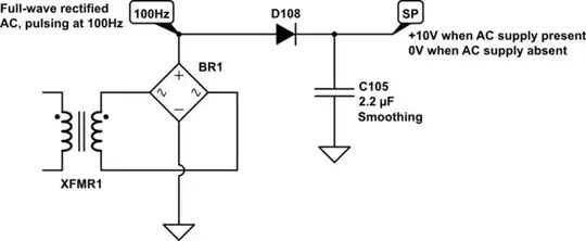
The other resistors and diodes you mentioned form small subsystems, which again have to be redrawn to be understood. Start with D108 and C105:

schematic

simulate this circuit

D108 and C105 form another small rectifier with smoothing capacitor. When AC is present, the "100Hz" node has the potential shown in the first graph above. C105 charges up to a steady +10V (approximately) on each incoming pulse. When AC goes away, C105 discharges, and SP falls to 0V. This is used as a signal to indicate the presence of AC power.

R102, R103 and D107:

schematic

simulate this circuit

The 10V pulses at node "100Hz" cannot be directly applied to the input of U102, without damaging it. R102 and D107 together form a clamp, preventing the potential applied to U102 from rising above +4.7V. They convert a 10V signal into a roughly 5V signal compatible with U102. I am not sure what R103 is for, I believe the circuit would function perfectly without it.

Simon Fitch
  • 27,759
  • 2
  • 16
  • 87
  • Thank you so much for your answer :D Also, to simulate your circuits which software do you use please ? Because i have LTSpice but it's not very intuitive for students. So for the capacitor C101, if i have a huge capacitor like 2000 uF for example it will work too ? Because the signal will be much smoother for the regulator ? For the diode OR, I understand that it works like an OR gate but why it's not simply connected to the 1 Hz output ? For R102 you mentioned above, how you choose the value ? Because i understand that it need a 5V input with low current to not burn the zener – Anthox Jun 28 '23 at 14:35
  • @Anthox Diode OR because you can't connect two logic outputs together (unless they are open-collector, these are not). You can make C101 is big as needed to reduce ripple as much as you need. No bigger, though, because inrush current becomes a problem. The main reason for large C101 is to prevent S falling below the minimum required for the regulator, probably about 8V for the 7805. You need to do the math, or run a simulation, or build the circuit and measure S with an oscilloscope to know if C101 is big enough. – Simon Fitch Jun 28 '23 at 16:35
  • @Anthox R102 is pretty arbitrary. Lower than 1k and current is unnecessarily large, higher than 100k and perhaps interference becomes an issue. 4.7k is a good compromise, setting current at about 1mA through R102. It could be 47k (and R103 scaled up by a similar factor) , and it would still work. It is not critical, unless these are TTL ICs, which have current-hungry inputs. CMOS IC inputs require almost no current, so even 100k would be OK. – Simon Fitch Jun 28 '23 at 16:40
  • @Anthox I used CircuitLab (https://circuitlab.com) to do all those simulations and graphs. It's very easy to use. It's also integrated into this SE site. The very first circuit in this answer works in the simulator. Click the "simulate this circuit" link underneath it, and that opens the design on the CircuitLab site, where you can edit and simulate. For fastser simulation, using more realistic component models, I use ngspice, which comes with the KiCad EDA package. They are both free, full-featured and open-source. – Simon Fitch Jun 28 '23 at 16:43
  • Ok thanks i will look at these tools – Anthox Jun 29 '23 at 23:02
0

Last part first: C103 and C104 are part of the quartz crystal resonant feedback circuit, and match the values that the crystal was tested with at its final manufacturing (fine tuning) stage. R104 is probably connected from output of a CMOS inverter to its input, and biases the input (in a logic-margin violation) for linear gain, to create an oscillation condition.

C101 is the main power-storage capacitor, that keeps the DC-electricity power flowing when the AC-electricity source is at zero volts (which happens every 10 milliseconds in a country that runs on 50 Hz electricity). It is sized so that enough charge is stored, and enough voltage maintained, to keep the regulator (U101) supplied with the power it requires to deliver the +5V that runs most of the clock circuitry. It is common practice to oversize that component, because any lapse in that power output will reset the clock; in this device, D106 provides backup power as well.

The D111 and D110 diodes, and R105, implement a crude OR logic function, requiring only small-signal rectification. R101 and R102 are current limiting so that D109 and D107, respectively, do not get warm. R103 makes sure that the clock signal (from the rectified AC source) goes LOW, to near ground, between cycles; the rectifiers alone will charge it up, but not discharge it.

D108 and C105 ensure that the Power_OK signal does NOT go low between cycles.

Whit3rd
  • 7,177
  • 22
  • 27
  • Thanks for you explanations, now it's much clear for me :) – Anthox Jun 28 '23 at 14:39
  • So to understand correctly, you said that R103 discharge the pin for clock. So it acts like a pull down resistor ? But how the value is chosen ? Thanks – Anthox Jun 28 '23 at 14:40
  • @Anthox The value of R102 is only critical if the clock it is connected to requires a fast downward transition (and that in turn depends on the capacitance of the pin which it discharges, and the leakage of diodes). It isn't critical for power dissipation. In some CMOS guidelines, 4k ohms is a "fast enough for all purposes" pulldown resistor, which would also work. – Whit3rd Jun 30 '23 at 05:54