You probably need to review potential, and what it means. As a reminder:
Voltage across something (for instance a base-emitter junction) is the difference between potentials at two different points in a circuit (base and emitter, for instance). Because this a difference, the voltage "across" or "between two points", is independent of any other potential anywhere else. The two nodes in question could have potentials +1000000V and +1000001V, or -0.5V and +0.5V, the difference is the same, 1V.
Voltage at some point in a circuit is the potential difference between that point and some arbitrarily chosen "ground", or "zero volts" node.
This means that you have to be careful how you use phrase statements about voltage (potential). If you say "across" a thing or "between" two points, or perhaps "over" a thing, everybody knows what you mean - the difference in potential between the ends of the thing. So if you say "the voltage between A and B is ...", you are stating how different A is from B, the value of A relative to B.
If you say the voltage or potential "at", or "of", some (single) point, then people will assume you've defined a ground somewhere else, and that's the zero-point, relative to which you quoted this potential. So essentially, saying "the potential at X is...", you are still quoting a potential difference between two points, but one of those two points has zero potential. The other, X, is an "absolute" potential relative to zero.
I'll give you an example:
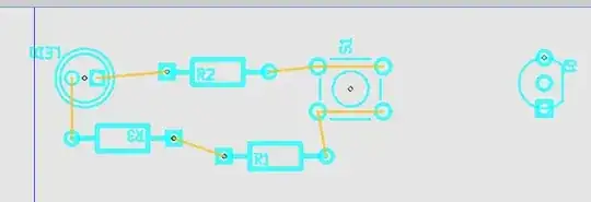
simulate this circuit – Schematic created using CircuitLab
Here I am able to make the following true statements:
The voltage across R1 is 2.3V
The voltage across R2 is 4.6V
The potential at S is +12V
The voltage at node C is +7.4V, or
The potential of C is 7.4V above ground, or
Node C is 4.6V less than S
The potential difference between B and E is 0.7V
The voltage across the base-emitter junction of Q1 is 0.7V
The potential difference between the collector and emitter of Q1 is \$V_{CE}=5.1V\$
As long as your descriptions are consistent with these ideas of absolute and difference, people will know exactly what you mean, and more importantly, if the people writing books are careful in this way, you will be able to understand them.
The book says that for NPN transistors the Base voltage (I'm assuming between Base and GND) has to be larger than the voltage at the Emitter (Again I think between GND)
The book says that base potential must be greater than emitter potential. These are both absolute potentials, and the statement implies \$V_B > V_E\$. You said you assume this is relative to ground, and you assume correctly. Absolute potentials are actually just potential differences between some node and 0V.
If the book had said "The potential difference between base and emitter must be greater than zero", instead, which means \$(V_B - V_E) > 0\$, this is saying the exact same thing.
The base-emitter junction can never have more than 0.7V across it, \$V_B - V_E \le +0.7V\$. When that difference is near +0.7V, then the transistor is on. Let's see if in my example above this is the case. Firstly, \$V_B=+3.0V\$, a statement saying that the base has a potential of 3V above our zero-volt ground. The emitter has a potential of \$V_E=+2.3V\$. The base is higher in potential than the emitter, the difference being \$V_{BE} = V_B - V_E = (+3.0V) - (+2.3V) = +0.7V\$.
Yes, this transistor is on.
There are two ways to switch it off. Either lower \$V_B\$ while keeping \$V_E\$ unchanged, or raise \$V_E\$ while keeping \$V_B\$ unchanged. Notice that both these actions would produce the same effect, to reduce \$V_{BE}\$ the potential difference \$V_B - V_E\$.
If there is a positive potential difference across the base-emitter junction (\$V_B - V_E > 0\$), there will be current through that junction. The emitter could be at −1000V, as long as the base is at −999.999V or above,
that junction is forward biased, and current will flow. How much current depends on the difference, and is independent of potentials anywhere else in the system.
When reverse biased, the junction will block current (it's just a diode, after all). That is, with \$V_E=-1000V\$, if \$V_B\le-1000V\$ then no current will flow. I hope you see that it doesn't matter what the emitter is connected to, or what its potential is. Base current depends only on the potential of the base relative to emitter potential. It's just the difference \$V_B-V_E\$ that determine base current.
Collector current is limited by the power supply voltage, and all impedances across that supply in the path down through the collector and emitter. In my example above it is the 12V supply, and R1 and R2 that define maximum collector current.
As long as you haven't reached that maximum (the transistor is not saturated), then the transistor will have a base current according to the relationship \$I_C = \beta I_B\$. That is, it is amplifying. The subject is huge, so that's all I'll say about it here.
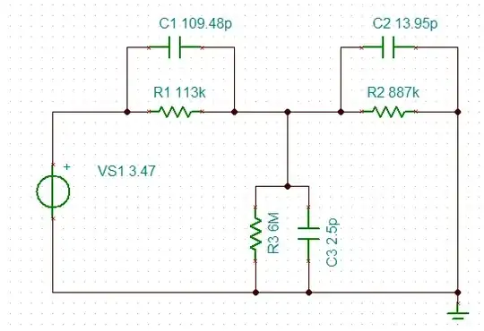
PNP transistors are the polar opposites of NPN. All the potential differences are reversed (\$V_{BE}=-0.7V\$, for instance), and currents flow in the opposite direction (emitter to collector). I'll redraw my circuit from above to illustrate the use of a PNP transistor to obtain the same behaviour:
simulate this circuit
I swapped R1 and R2, so that R1 remains at the emitter, and I moved voltage source V2 to produce a potential 3V lower than the positive supply, +12V (as opposed to 3V greater than 0V from before). This sets base potential to +9V, and obtains a base-emitter potential difference:
$$ V_{BE} = V_B - V_E = (+9.0V) - (+9.7V) = -0.7V $$
Also, I inverted VM1. That's because I want to remain consistent with the naming conventions of potential differences in transistors. People often refer to parameter \$V_{CE}\$, which to be technically correct is defined as \$V_{CE}=V_C-V_E\$. Since collector and emitter have been swapped, I inverted VM1 to produce the correct sign:
$$ V_{CE}= V_C - V_E = (+4.6) - (+9.7) = -5.1V $$


