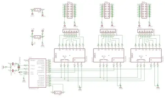
I am working now for a while with bias calculations. I have found a good turorial to calculate it by my own and I have seen that there are already calculators on internet, which made my life much easier than i supposed to manage. I have now a circuit below. This is one is a good one, I think so. I used a pre-amplifier, after that boosted it and finally used a differential amplifier with pre-configured bias. I used this calculator and can be found on, "https://www.daycounter.com/Calculators/Differential/Differential-Amp-Calculator.phtml". As I predicted on former post of "Amplifier gain values vary when changing power supply" that I need an amplifier that works in reliable conditions. This amplifier should serve as a RF amplifier and in the end a LM386 audio amplifier will amplify the sound of this transmitting which is also 200 times amplifying. Can you tell me if I am on the right way and can this be used for RF amplifications. The circuit amplifies at 8MHz an 1uV amplitude about 500-600 times as shown below. Can the components be soldered properly with these values. I tested them in LTSpice.
-
I would lovely send you the LTSpice file with .asc extension. So you do not have to integrate all these parts manually to simulate this circuit at home or work. Sorry. – lastime Jun 12 '23 at 18:52
-
2The BE junction of Q5 not allow to swing the voltage of Q5 collector. It will clamp it to 0.7V. – Michal Podmanický Jun 12 '23 at 21:40
1 Answers
Unfortunately, you fell into a bit of a trap here - biasing circuits like the one you've built for Q5 and Q6 might seem to "work" in a simulation, but in practice they'll just saturate at either the supply voltage or at ground. The same goes for the biasing scheme of Q1 and Q2.
The reason for that is the imperfect matching of the physical transistors that you can actually buy. In your case, the thing that's going to get you is the transistors' imperfectly matched base-emitter voltage.
Let's take the Q5/Q6 pair as an example. You're biasing Q5 in such a way that its collector-emitter and base-emitter voltages are equal when the circuit is quiescent; the current through Q5 is determined by R11. This is valid and will work. Q6, however, will not be particularly happy about this. Its base-emitter voltage is equal to the collector-emitter (and therefore base-emitter) voltage of Q5. Ideally, this would cause the same current to flow through Q6 as through Q5, and this is roughly what happens in the simulation because their base-emitter voltages are equal. Unfortunately, this only works as long as Q5 and Q6 are exactly identical, which is not true for real, physical transistors - it's only true in the simulation. If Q6 has only slightly different properties, the current flowing through it will be dramatically higher or lower, causing your amplifier to saturate and malfunction.
As an example, Q5 might need 600mV between base and emitter to pass the required ~0.5mA, while Q6 might only need 580mV to pass the same current. When you then apply 600mV to Q6, it might want to pass something like 2mA, which it can't due to R14, causing it to just fully turn on and ground its collector. Your amplifier won't amplify much.
The base-emitter voltage will also change dramatically with temperature, which means that the circuit might work for a few seconds and then malfunction when it begins to heat up. It's even worse when different transistors in the circuit heat up to different temperatures as that will cause their properties to diverge even more.
To fix this, you should build your circuit in such a way that it's insensitive to variations in the transistors' properties. Since you only want to amplify high frequencies, you could limit the circuit's DC gain to make it easier to set its quiescent point, and only raise its gain at higher frequencies.
Here's an example of such an amplifier stage:

simulate this circuit – Schematic created using CircuitLab
This circuit only has an inverting gain of 1 at DC due to the negative feedback created by R3. This makes it very easy to set the quiescent point - a simple resistive divider, consisting of R4 and R5, does the trick just fine. At high frequencies, though, R3 gets shorted out by C1, essentially turning it into a grounded-emitter amplifier.
The voltage at the transistor's base will be approximately 1.6V (a third of 5V), which means that the voltage at its emitter will be roughly 1V. This causes 0.3mA to flow through R3, which in turn flows through the transistor and through R2. This again causes a 1V drop across R2, which means that the output voltage is 4V when the amplifier stage is quiescent. The collector-emitter voltage of the transistor will therefore be 3V (difference between 4V at the collector and 1V at the emitter). Its AC gain will be very high - it's only limited by the transistor's parasitic elements (Early effect and, at high frequencies, parasitic capacities).
This amplifier stage can be cascaded as many times as you want, you just need an AC coupling capacitor in front of each one (C2 in the schematic). Note that you might have to use a faster transistor than the BC546B that you've used in your simulation as that particular transistor is really only meant for sub-1MHz applications and won't amplify much at higher frequencies. You can of course still try it with the BC546B but the results likely won't be that great.
- 14,865
- 28
- 50

