0

Looking for a way to fully shutdown a DC-DC boost converter.

Searching around the web I have found this solution which recommends putting a MOSFET on the input side of the converter in order to kill the input voltage: How to fully shutdown a boost converter?

Issue I have is that in my case, I have very limited amount of space and having MOSFET on input requires it to handle fairy large current which means a fairly beefy package.

I was thinking of having a P-MOSFET on the output (after bulk caps) instead which is then ENABLED/DISABLE by a micro.

Any reason why the input side MOSFET seems to be the most recommended solution (answer above and internet in general) and anything else I should consider before putting the MOSFET on the output.

Zygis
  • 58
  • 6
  • If a redesign is an option to you, there are boost converter ICs with output disconnect built in. – winny May 30 '23 at 10:25
  • @winny Unfortunately it is not. I have what I have and I need the output voltage to disappear completely when the micro decides that. Converter in question is LM5123 in case that is somehow relevant. Has shutdown but it just disables the internals, not the output. – Zygis May 30 '23 at 10:27
  • I see. What's your input voltage (range) and output voltage and current? – winny May 30 '23 at 10:39
  • @winny Input 9-16V; Output 24V 1A max continuous. – Zygis May 30 '23 at 10:45
  • 2
    There are several reasons you what to disconnect the input, one of them being that you minimise power losses when you don't need any boost conversion. If you just disconnect the ouput you keep the booster going anyway and there will be some continuous (albeit small) power losses. I would look at choosing a very low Rd-s P-MOSFET in the smallest package you can find. There should be plenty of P-MOSFETS with 10m - 30m Ohms Rds-on available in very small packages (say SC-79 or equivalent). – citizen May 30 '23 at 10:57
  • 2
    Moreover on what @citizen already said, switching the input would also allow your boost converter to regulate away the voltage drop from your P MOSFET. – winny May 30 '23 at 11:01
  • @citizen Thank you. The regulator has the internal shutdown which brings it down to 3uA (according to data sheet), I couldn't care less about this amount of wasted power in this application. I expect the micro to put the converter into shutdown and disable the output with a MOSFET. SC-79 appears to be a 2 pin package? Components packed on both sides of the board it is quite bad and I would struggle to squeeze in any more in. Apart from wasted power, what other considerations are there? – Zygis May 30 '23 at 11:11
  • @winny can I not just move the voltage sense after the MOSFET to account for the additional drop? Also probably going drop even more over connectors and wires, not sure if additional 50mV is that concerning even if I were to leave it as is. – Zygis May 30 '23 at 11:11
  • @Zygis. In your current configuration your input will stay connected to the output, so I wasn't refering to the losses incured from the 3uA in shutdwon mode. As winny suggested there is also the benefit of the regulation compensating for the slight voltage drop on the input ! The SC-79-3 or SC-79-6 etc are 3 pin and 6 pin packages, but there are also the SC-70-3, SOT323-3 etc and even the micro-FOOT packages to suit your fancy ! – citizen May 30 '23 at 11:20
  • @Zygis Probably, but if you want to do minimum changes to your existing design, switching on the input would be easier. If you are going to rip apart your design, I would suggest to go for a boost converter with output disconnect built in. – winny May 30 '23 at 11:29
  • @winny Not really minimum if I have to rearrange the whole input side to make room for additional components. Have enough room on the output for a D-PAK without touching anything else. So far from your and [citizen] comments I can see that the only concern raised seems to be some (extremely negligible) power wasted by the converter being in the shutdown and whatever leaks through the MOSFET to the load while it is off. MOSFET on the output will drop a bit of voltage while ON, but again, not much a concern in this case. Is that all there is to this decision/trade-off? – Zygis May 30 '23 at 11:39
  • @Zygis. It sounds like you really have no choice then. If you can't even fit in a mirco-FOOT on the input then you're done choosing. Only choice left is a TO-92 on the output ;-) – citizen May 30 '23 at 11:42
  • @citizen Not that extreme, but yeah. the input side is bad and this was an oversight in the design. Need to fix it now. If either of you could type up an answer I'll accept it. – Zygis May 30 '23 at 11:44

1 Answers1

2

First of all, using the ENABLE/DISABLE feature of the chip cannot be a solution here because even if the switching stops the output will be equal to the input voltage (neglecting body diode drop).


I was thinking of having a P-MOSFET on the output (after bulk caps) instead which is then ENABLED/DISABLE by a micro.

Well, this is a solution. The current flow on output side is lower than that on input side, so this allows you to select a smaller MOSFET. So yes, can be acceptable.


... anything else I should consider before putting the MOSFET on the output.

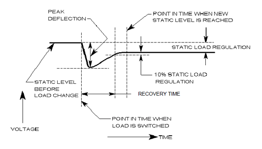
One other thing to consider here is the recovery behaviour of the converter output. Because the converter will keep running and the output will always be present (before the load), once the load is re-connected across the output the instant output current rise (i.e. step load change) will cause the output drop by some amount and then recover. This recovery, depending on the design (including compensation) and the load itself, may take too long or even may be oscillatory.

Similarly, once you disconnect the load, depending on the load state and design (again), the output will overshoot by some amount and recover. This overshoot amount may or may not be acceptable.

So you may want to check if the output voltage variation (drop amount or overshoot amount) and load behaviour under these states is acceptable.

Also the converter will keep running so the consumption will be high but depending on your application this may not be of a concern.


Any reason why the input side MOSFET seems to be the most recommended solution

Cutting either input or output is similar in terms of electrical design and simplicity (neglecting sizing the switch). Either a PMOS or a load switch IC will work but I personally recommend a load switch IC here as it's way simpler and some of them have built in over-current and thermal protection which might be quite useful.

Another advantage is that, unlike the dynamic behaviour that I tried to explain above, the load will take advantage of the soft-start feature of the IC so the output will rise from zero to its nominal gradually, and with almost no overshoot (hopefully). So, starting the converter loaded becomes less problematic.

Rohat Kılıç
  • 26,954
  • 3
  • 25
  • 67
  • 1
    Thanks for the additional considerations. Marking this as answered as it captures previous points from others and add more information. – Zygis May 31 '23 at 09:07