2

I am working with the attached circuit, sourced from here: Original

This circuit is designed for a single sided power supply and has worked very well for me in the past. For a new project, I would like to use it with a dual sided power supply, providing -6V, 0V, and +6V. Ignore the "precharge" section in the dotted box and R1, they will not be used.

  1. I think I can remove R3, R4, R5, and C2 because they are just used to bias the op-amp for a single sided supply. Is this correct?
  2. I don't understand the purpose of C4. Why is it there and is it required for a dual sided supply?
  3. I don't understand the purpose of D2. Why is it there and is it required for a dual sided supply?
  4. Would I be correct to connect each of the ground symbols, except for the U1 (-) power supply and the decoupling cap(s), to my 0V rail after removing the bias components I described in item 1?

Thanks!

AGC Schematic

UPDATE:

Breadboarded the circuit based on the feedback received.

All of the ground locations were connected to -6V except for R3 which was connected between U1 pin 3 and 0V.

R4, R5, and C2 were eliminated.

Initially I tried eliminating C4, but circuit oscillated badly. I replaced C4 and connected that between R6 and -6V. After that the circuit seems to be working well.

Telluride
  • 45
  • 4

2 Answers2

3

Would I be correct to connect each of the ground symbols, except for the U1 (-) power supply and the decoupling cap(s), to my -6V rail after removing the bias components I described in item 1?

Why not connect U1's negative supply also to -6V? The op-amp's supplies will have to be +6V and -6V for your idea to work, but you are otherwise correct.

I don't understand the purpose of C4. Why is it there and is it required for a dual sided supply?

C4 has high impedance at DC, which is as if it's not there, for any DC component of the signal. C4, C7 and R6 can be disregarded at DC, leaving only R7, which makes U1 a voltage follower, with unity gain for any DC offset present at its non-inverting input. U1's output is therefore centered about whatever mean potential is established by the biasing network of C1, C2, R3, R4 and R5.

Another way of thinking about C4 is to consider its DC charge state. It will develop a mean DC voltage equal to the mean output potential, raising the op-amp's inverting input potential to equal the mean potential at the non-inverting input. In this way it becomes a kind of "ground" reference at about +6V, instead of 0V.

C4 will not be required if you have an actual 0V node, as indeed will be the case if you convert to supplies with +6V, 0V and -6V.

I don't understand the purpose of D2. Why is it there and is it required for a dual sided supply?

D2 prevents Q2's base from dropping below -0.7V, and Q2's base-emitter junction prevents that potential from rising above +0.7V. Between them Q2 and D2 constrain the signal at Q2's base to be within +0.7V and -0.7V.

There are two consequences that spring to mind, there may be others. Firstly, Q2's base-emitter junction will never be reverse biased to the point that it breaks down, which would seriously mess up the AGC's behaviour.

Secondly, the right side of C5 experiences similar loading during both negative and positive excursions of the op-amp's output. If D2 were not there, the resulting loading asymmetry would offset the mean potential at C5's right end, which should be 0V in the original, or -6V with your modifications.

You can't remove D2.

I think I can remove R3, R4, R5, and C2 because they are just used to bias the op-amp for a single sided supply. Is this correct?

You are almost correct. You will still need R3 to bias the non-inverting input at 0V, but the other three elements can be removed.

What you are left with is:
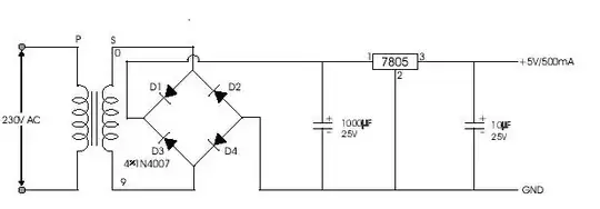
schematic

simulate this circuit – Schematic created using CircuitLab

All gain control elements, that I've omitted here, need to operate around -6V, their "grounds" must become -6V. All their +12V nodes become +6V.

Since your output is now ground referenced, and the AGC system requires a -6V baseline signal, C5 can no longer be used for DC blocking in both roles. It may no longer be required to block DC for the final output, but C5 is still necessary to allow the signal at Q2's base to be centered around -6V. Hence C5's change of position.

It's not clear to me without more thinking, whether it's safe to raise the input bias (via R1) to 0V, instead of -6V, so I've left it biased as it would have been in the original. Since the source is a microphone, that may be good enough, but if the source wasn't isolated, and shared a common 0V with this module, then additional AC coupling (a capacitor) at the input would probably be necessary.
Simon Fitch
  • 27,759
  • 2
  • 16
  • 87
  • I marked this as the correct answer after finally having a chance to breadboard the circuit, thank you! The only thing I found was that C4 could not be eliminated even when I connected R6 to my 0V reference. I connected C4 between R6 and -6V and it worked correctly. The output was somewhat unstable with the 47uF cap, but it looked really good when using a 22nF cap. My test signal was 7.1kHz. I am not sure if this is an artifact of my less than ideal layout on a breadboard, or something else. I appreciate the help! – Telluride Jun 03 '23 at 03:48
3

I think I can remove R3, R4, R5, and C2 because they are just used to bias the op-amp for a single sided supply. Is this correct?

Yes. But you need to 'bias' the input to ground. The most compatible way to do this is keep R3 and connect its lower end to ground instead of R4 and R5.

I don't understand the purpose of C4. Why is it there and is it required for a dual sided supply?

C4 and R6 form a high pass RC filter that reduces op amp gain to 1 at DC. This makes it less sensitive to input offset voltage, and attenuates very low frequencies that could affect the AGC function.

I don't understand the purpose of D2. Why is it there and is it required for a dual sided supply?

On positive halves of the AC audio output Q2's Base-Emitter junction conducts. On negative halves it doesn't. This cause C5 to build up a negative charge that cuts the transistor off. The diode conducts during negative halves to make the loading symmetrical.

It also prevents the Base-Emitter voltage going below -7 V which would cause the junction to act like a Zener, though in this case that probably wouldn't harm it.

If you replace C5 with a short then D2 isn't necessary. You can do this because with the input biased to ground the output should also center around ground (+- input offset voltage, which should be insignificant).

Would I be correct to connect each of the ground symbols, except for the U1 (-) power supply and the decoupling cap(s), to my -6V rail after removing the bias components I described in item 1?

No. The only connection you should make to -6 V is U1 pin 4. Since the precharge ciruit will be powered by +6 V instead of +12 V, you should replace R16 with a short to maintain the correct bias voltage. R15 should be reduced to ~50 kΩ for the same power on mute time, and R9 should be reduced to ~500 kΩ to maintain the recovery time.

Due to the lack of voltage bias, C4 should be replaced with a non-polarized capacitor.

This should make the circuit act similarly to the original, but it may not be identical due the lower voltage in the AGC part. Some fine tuning might be necessary.

Bruce Abbott
  • 55,540
  • 1
  • 47
  • 89