I never thought of that!
However, the I3 and I4 current sources have their own \$VDS_{SAT}\$ associated with them (or their own compliance voltage) above ground. Therefore, your "bias" point is located at a \$VDS_{SAT}+V_{gs,M1}\$ above ground. The DC operating points required for both do not match by a \$V_{gs,M1}\$ term, because the voltage the sources of your input pair is at \$VDS_{SAT}\$ only.
Now, you can make I5 as a cascode, so you have \$2VDS_{SAT}\$, but then your voltages wouldn't match by a \$V_{th}\$ term, and you still need to generate a bias voltage for the cascode...
This doesn't mean it'll never work, but you'll have some biasing problems there that might get you in trouble.

The basic reason why this would be frowned upon, criticized, and probably not robust within an IC is for the reasons I exposed above. All 3 current sources (I3-I5) would be implemented as 3 transistors, they need high overdrive in order to be good current sources. If you connect as you do, you're basically saying that \$V_{ds,I5}\$ is eequal to \${V_{ds,I3}+ V_{gs,M1}\$. In an IC, the drain source voltages across transistors will not change by a lot, specially in deep-submicron. One vdsat could be 200mV and another one could be 250mV. There might be larger differences, but no one will rely on those because they change from PVT to PVT corner.
And sometimes it might work, but then you have to look at the margins (the difference between overdrive voltage and vds) of each transistor. If this margin is small, then this is not robust enough as process variations or any other imperfection might drive it out of saturation easily. In 28nm I typically hit for ~100mV-150mV of margin (my supply is typically 0.9V).
If you implement I3 and I5 as resistor, then you have a degree of freedom there to size your output DC voltage such that, when added to the \$V_{gs,M1}\$, you'll have approximately the same voltage at the top of I5. Then, connecting shorting both nodes could work biasing-wise.
Finally, I also add what I said in the comments below, the sources of your input stage now have an extra parasitic capacitance connected in series with your I3 and I4. Might generate some parasitic pole and might also hamper your CMRR at high frequencies. As the other answerer wrote, your PSRR from ground to signal might be hampered if you implement those I3-I4 current sources, a current source will ideally keep the outputs stable (provided there's common-mode feedback if using a differential output), while a resistor will not.
EDIT:
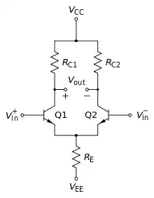
I don't know if you mean this, but you have a differential output voltage. If that's how you want to design this, you need a common-mode feedback circuit that takes the average of your outputs can control the bottom current sources.


