Here are my thoughts after taking a good look at the diamond buffer.
To simplify things, I'll assume a load at the output is sinking current to ground, so that the lower half (the "pushing" part? I never know which is doing the pulling, and which is pushing) is idle when the input is positive. We can ignore that lower half for now, and focus on the upper "pulling" section.
I'll compare two approaches to driving the base of the output transistor (Q2 below), both of which apply an offset of +0.7V to the input potential, to eliminate crossover distortion:

simulate this circuit – Schematic created using CircuitLab
Q2 is operating as an emitter follower, whose potential at OUT is 0.7V lower than its base, due to its base-emitter junction having 0.7V across it.
Above left, a +0.7V input offset is achieved using diode D1. R1's purpose is to provide a source of current for D1, so that it can develop the required 0.7V potential difference. It must also source all base current necessary for any load current, drawn from Q2's emitter.
On the right, the +0.7V offset is produced by the base-emitter junction of Q1 (note that it's PNP). This time R1 is also replaced by a constant current source, which acts as a "load" for Q1 to form another emitter follower. I'll discuss the benefits of using a current source later, but just be aware for now that like R1, it must simultaneously source enough base current for Q2 and emitter current for Q1, under all circumstances.
In both cases, the combined offsets of +0.7V from D1/Q1 and −0.7V from Q2 cause OUT and IN to have roughly the same potential, effectively overcoming most of the input "dead zone" between 0V and +0.7V that would be present without D1/Q1, and which would be responsible for crossover distortion in a complete push-pull arrangement.
Current through R1 (above left) must be sunk either via Q2's base, or by the input voltage source V1. Which way it goes depends on the load. In this next example I'm using the circuit above left, and loading the output to draw either 2A (left) or 0.2A (right). I've set Q2 to have \$\beta\approx 100\$, and I am applying a 5V input:

simulate this circuit
I've chosen R1 such that in both those circuits current through it is fixed at a little under 20mA (since the voltage across R1 is fixed too), but that current splits into two paths. Either it is sunk by the base of Q2, or by D1 and V1, and the proportion of that 20mA total in each path is dependent entirely on severity of the load. There are a few noteworthy points:
Under low output load, almost all R1's current flows via D1, to be sunk by V1. Under high load, much of that current is diverted into Q2's base instead.
The diode is a less than ideal way to get a 0.7V offset (see VM2). The actual offset that it produces varies wildly (150mV change here) with variation in load, since the current through it varies wildly. This could be mitigated a lot by using a diode-connected transistor instead of a diode.
Output potential varies at least as much as D1's potential difference.
V1 is required to sink up to 20mA, too much to ask of a typical op-amp.
These are failings that the diamond buffer aims to resolve, by using an emitter follower Q1 instead of diode D1. I'll leave R1 in place, without addressing the current source just yet. Here are the same load scenarios, but with Q1 replacing D1:

simulate this circuit
Notice that:
Input offset goes from 770mV to 660mV, a change of 110mV between loads. A small improvement, not as dramatic as I had anticipated.
Input source V1 is sinking well under 1mA, a huge improvement. That's because almost all R1's current is being sunk into via Q1's emitter to ground. The combined current gain of Q1 and Q2 is many thousands, and so demand for current from V1 will be commensurately small.
This is a perfectly acceptable load on an op-amp output.
Already that's a big improvement, but there's more; we still have to talk about current source I1. To understand why it's a good thing, start by understanding the limitations of using resistance R1. Remember that R1 is the only source of base current for Q2. Q2's base potential can't rise any higher than R1 can "pull" it. R1 introduces a constraint to Q2's maximum possible base current, and therefore also maximum collector and emitter current.
In the above examples, I chose R1 to be able to provide 20mA of base current for Q2, but when the load requires more than \$\beta_{Q2} \times 20mA = 2A\$, that value for R1 is clearly too high. If we raised \$V_{IN}\$ any further, the voltage across R1 must reduce, and the current through it will eventually fall to the point where it provides insufficient base current for Q2 to stay on.
Let's take a look at what happens to the output of the above circuit as I sweep input potential from 0V upwards:

R1 places a huge constraint on the current our circuit can provide to its load, 2A in this case. And with our load of 2.5Ω that current limit prevents the output from ever exceeding 5V.
This is what happens when we set our input to 12V, for a 12V output, but we sweep the load current upwards from 0A:

It's a lovely current limited voltage source, which might be exactly what you need, but here I am interested in how R1 can be problematic. Making R1 smaller will raise the maximum base current available to Q2, which, on its face is fine, but by doing so you increase quiescent current through Q1, when the load is small, or input potential is low. I've lowered R1 to 115Ω here (the reason for which is explained below):

simulate this circuit
There's more than 120mA flowing through Q1, even with zero input, and negligible output current. Considering that Q2's base doesn't ever require or draw more than 20mA (assuming we never need more than 2A out, \$I_{B(MAX)}\approx\frac{I_{E(MAX)}}{\beta}=\frac{2A}{100}=20mA\$), this is 100mA more than we need. Quite the waste.
A little algebra should clarify this. If our supply potential is \$V_S\$ and input potential is \$V_{IN}\$ then by KVL the voltage \$V_{R1}\$ across R1 is:
$$ V_{R1} = V_S - V_{BE} - V_{IN} $$
Mr. Ohm tells us the current \$I_1\$ through R1:
$$ I_1 = \frac{V_S - V_{BE} - V_{IN}}{R_1} $$
Maximum output current will be a little less than:
$$
\begin{aligned}
I_{OUT(MAX)} &\approx \beta_{Q2} I_1 \\ \\
&\approx \beta_{Q2} \frac{V_S - V_{IN} - V_{BE}}{R_1}
\end{aligned}
$$
However, to see the real problem with R1 we must consider not only the current through it for maximum load, but also with zero input, because that's when the voltage across R1 is at its greatest. So, lets find a value for R1 which satisfies a need for 2A maximum output current when the output is 12V, for instance:
$$
\begin{aligned}
R_1 &= \beta_{Q2} \frac{V_S - V_{BE} - V_{IN}}{I_{OUT(MAX)}} \\ \\
&= 100 \frac{15V - 0.7V - 12V}{2A} \\ \\
&= 115\Omega
\end{aligned}
$$
And now lets see what quiescent current flows with zero input:
$$
\begin{aligned}
I_1 &= \frac{V_S - V_{BE} - V_{IN}}{R_1} \\ \\
&= \frac{15 - 0.7V - 0}{115} \\ \\
&= 124mA
\end{aligned}
$$
That's a lot of current, considering only a maximum 20mA of it will ever flow into Q2's base. As i said, what a waste.
Since lowering R1 isn't a great idea, what if we replaced it with a current source of a little over 20mA, say 25mA? That way 20mA is always available for Q2's base (enough for our required output current of 2A maximum, \$\beta \times 20mA = 2A\$), and any current that doesn't flow there is left over to operate the emitter follower of Q1:

simulate this circuit
Problem solved. Quiescent current is fixed at 25mA, Q2's base is never starved of current, and there's a little left over for Q1.
Unlike R1, the current source also enables the base of Q2 to reach potentials very near the supply, meaning that the only reason the output would be voltage-constrained is if Q2's base current demand is more than I1 can provide.
By lowering I1's current, you limit maximum base current for Q2, which places a cap on maximum output current. Obviously it relies heavily on \$\beta\$, but this could be way to prevent an output short-circuit from destroying things.
It remains to make a complete, practical push-pull stage, using these values, and see how it performs.

simulate this circuit
I've had to employ the usual trick of emitter degeneration with R5 and R6, biasing Q2 and Q4 slightly more "off" to reduce their quiescent current. That will naturally reduce gain somewhat under load:

That's nice, no crossover distortion, very wide output voltage swing, beginning to clip a little past 12V. If I replace RL with 3Ω that will double the load current, and we should see Q2 and Q4 get starved of base current at about 6V or so:

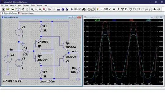
The diamond buffer. Pretty neat.
