17

I've been spending time with schematics debugging busted 1970s TTL-based computing circuits. I'm sure this is a more general question but I'll ask it in this context since that's what I'm exposed to.

Why is so much TTL circuitry designed around negative logic, such that low signals indicate "true"? This shows up primarily in the most typical 74xx series gates being NAND and NOR, which results in a spaghetti nest of difficult-to-intuit signals within the more complex circuits. Here's just one sample sheet from a disk controller. Obviously with boolean logic "it's all the same" in the end-- no scope of functionality is lost, but surely there's some reason that led to the primacy of the negative gates over designing around the far more intuitive positive-all-the-way-through logic.

enter image description here

Even when I understand the semantics of the inputs on the left and the outputs on the right, tracing how the former gets to the latter with common sense deductions of state changes gets pretty tricky!

This seems like a useful explanation for input signals to a circuit that are held high and dropped low only rarely to trigger something-- but in a nest of high frequency signals it seems hardly to apply.

Thanks.

BZo
  • 1,575
  • 1
  • 11
  • 22
  • 7
    that's called `active low` logic – jsotola Apr 17 '23 at 05:55
  • 2
    Like with all 'why did history go this way' questions, there is no one answer. There was however a mix of parsimony and the way physics worked for the devices at the time. When embedded in that negative logic mindset, it was no problem to see enables as being True when low, it was 'just how everything worked' and you got on with it. – Neil_UK Apr 17 '23 at 06:58

11 Answers11

21

One reason is simply power efficiency. A TTL input was a current source, would suck system power when it was LOW, but not when it was HIGH. So, you save (about 1.2) milliamps whenever you leave an inactive input in the HIGH state.

The later implementations (LS series) were lower power, but with dozens of chips, many inputs per chip, the power drawn from SN7404 inputs (1.2 mA each) held low, from a 5V supply is 24 * 6 * 0.0012 x 5 = 0.86 W

Whit3rd
  • 7,177
  • 22
  • 27
  • 7
    A small correction: the 1.2 mA current is distributed between the grounded inputs (the base-emitter junctions of the multiple-emitter transistor); i.e., it does not depend on the number of grounded inputs. In contrast, the currents of the inputs connected to Vcc are summed. – Circuit fantasist Apr 17 '23 at 09:09
  • 2
    @Circuitfantasist Well spotted! I'll change the example to SN7404 with six input transistors... – Whit3rd Apr 20 '23 at 07:03
12

The original SN5400/7400 logic was before my time, and I suspect most of those here.

One possible motivation is that the drive from high to low is about 40x stronger than the drive from low to high, so with capacitive loading and fanout the transition from high to low will be crisper. Hence it makes sense to clock flip-flops on the negative-going edge.

For example, this Fairchild 7400 datasheet shows a transition time of 22ns low-to-high and 15ns high-to-low with only 15pF loading.

The original 7400 gates were NAND and NOR (7400 and 7402) - 7401 and 7403 were open-collector. Gates like the 'AND' didn't come along until the 7408 and it was slower (27 and 19ns) because the internals required another stage effectively.

Commonly needed logic constructs such as AND-OR were efficiently implemented by all NAND gates.

A quite amazing reference is this 1967-68 TI databook, which contains detailed information on early TTL and DTL parts (clearly aimed mostly at military type applications). That's only 4 years or so after the first TTL parts were introduced. Unfortunately, in relation to this question, it has little to offer that I can see.

enter image description here

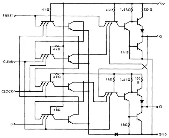
The simplicity of the internal schematic of the 7474 is striking, only 16 transistors per D flip-flop inclusive of the totem pole outputs (albeit six of them have a surfeit of emitters).

Spehro Pefhany
  • 376,485
  • 21
  • 320
  • 842
  • Your last point there strikes me as possibly particularly important-- that the NAND is a universal building block. – BZo Apr 17 '23 at 00:31
  • Yes, it is. So is a 2 input NOR. But that doesn't mean NANDs were used just for that reason. Parts count was a big issue in the 70's and 80's. You were not going implement a design using NANDs exclusively just because they are universal. You used a combinations of NANDs, NORs, ANDs, inverters, etc to implement your design with the fewest parts possible. – SteveSh Apr 17 '23 at 01:19
  • 2
    In fact, back in the late 70's, we had a Cray computer up at corporate headquarters that we could use to do logic/digital simulations of designs. These were SSI/MSI based designs. But the simulator was built around 3-input NAND gates (there's that universality point again). So board designs using SSI & MSI components had to be compiled into a netlist of 3-inputs NAND gates in order to run on the simulator. – SteveSh Apr 17 '23 at 01:26
  • @Spehro Pefhany - Your 40X stronger high to low comment is not consistent with your example from the Fairchild 7400 datasheet, that shows a transition time of 22ns low-to-high and 15ns high-to-low with only 15pF loading. – SteveSh Apr 17 '23 at 22:03
  • 1
    @SteveSh 16mA/0.4mA = 40 is probably what was meant. – devnull Apr 17 '23 at 22:12
  • 1
    @devnull - Ahhh, yes. that would make more sense. – SteveSh Apr 17 '23 at 22:18
10

Another reason may be a now-since-forgotten historical aspect: active-low circuitry is more fundamental to BJTs in general, and open-collector NPN logic -- whether discrete (lone transistors), or early families like RTL and DTL -- was the method of choice, requiring the least components. Indeed, many of these had outputs that could be wired in parallel to get a "free" OR function (hence "wired OR" -- in the active-low sense, that is).

TTL isn't wired-OR-able (unless specified!), but its NPN-only* design carries similar limitations. Hence the asymmetrical output impedance and voltage ranges, for example.

Perhaps interoperability with existing logic systems/families was such a consideration, contributing to the preference for active-low signals.

If nothing else, designers accustomed to active-low control signals will likely continue to use them, even if it isn't necessarily well justified (by physical reasons) to choose one polarity or the other. Add in even a tenuous degree of interoperability (e.g. early CMOS versions of CPUs, memories, etc. worked alongside TTL and NMOS parts) and you've got a strong reason to continue using it.

*I'm not actually sure offhand if PNPs were ever used (most likely the lateral variety?), but anyway, the basic input and output structures are all NPN.

Related: why NPN? They perform slightly better than PNP. PNP were actually more common really far back (e.g. alloy junction germanium), but NPN took over with the introduction of silicon transistors. The performance difference is pretty modest (~20%?); not like the ~2.5 ratio between PMOS and NMOS (which does still prefer active-low for physical reasons; but despite that ratio, it's actually a pretty minor preference in practice).

(Which begs the question: why was early MOS P-channel? Quirk of the earliest MOS processes, as I understand it. They pretty quickly went to NMOS (N-ch with resistor or FET pull-ups, analogous to RTL) when the process became available, and then CMOS.)

Tim Williams
  • 22,874
  • 1
  • 20
  • 71
  • 2
    I believe that NPN > PNP became true with the introduction of planar technology and the IC revolution. Lateral PNP (which iirc were introduced by Widlar, or was it Hoerni?) kind of sucked. – Sredni Vashtar Apr 17 '23 at 04:05
8

It's because with TTL and variations thereof (S, LS), an input has more noise immunity when the unasserted input is pulled to a high state (Vcc, Voh) than when it's pulled to a low state (GND, Vol). Hence we designers tended to make the unasserted state a logic 1 (high) and the asserted, or active state a logic 0.

TTL devices have an input low voltage level, Vil of 0.8 V (min), so that any input level less than that will be interpreted as a logic 0. TTL outputs have a guaranteed output low level Vol, of 0.4 V (max). So worst case you only have 0.4 V of worst case noise immunity in the low state, and 0.8 V best case (if the input were at 0 V, or GND)

The noise immunity for a high input is better than this. While the guaranteed noise immunity in the high state is the same (0.4 V), based on worst case Voh and Vih levels, in practice you're usually better than this as the Voh level may be closer to Vcc (depending on loading). With a Voh of close to 3.5 V (for Vcc=5.0 V) and Vih=2.0 V (max), this gives you abut 1.5 V of noise immunity in the high state.

EDIT 1

Note that on 54xx/74xx TTL devices like flip flops, counters, etc with reset (or clear) and set inputs, those inputs were almost always active low. Since you didn't want an errant noise glitch resetting a bunch of flip flops or counters, it is consistent with my argument above that keeping an active low input high when unasserted provided better noise immunity than the opposite.

SteveSh
  • 9,672
  • 2
  • 14
  • 31
  • 1
    I would just as well argue that the noise immunity is better in the low state: the bus is driven harder (lower impedance). Probably, given a mix of electric and magnetic [near field] interference sources, the levels chosen are a reasonable enough compromise, so it works out well enough in both states. – Tim Williams Apr 17 '23 at 00:07
  • So then, why do you think "negative logic" was used? At my former company, digital design guidelines going back to 1983 have recommended/required this practice. – SteveSh Apr 17 '23 at 00:20
  • Thanks. This may seem like a dumb followup, but if we like "asserted" to be the low state, then why are the inputs to the NAND not also inverted? My confusion stems from that fact that when you start combining a lot of logic, you end up flip flopping your "true" states as they move through the network of gates. THanks – BZo Apr 17 '23 at 00:33
  • @SteveSh Perhaps some contemporary design documents can be found; or some info in early databooks? Might be hard to find anymore, alas. I would guess the other answers carry more weight; but I don't have direct evidence such as above. Noise immunity might also be a stronger concern contrasted against predecessors i.e. RTL/DTL? – Tim Williams Apr 17 '23 at 00:42
  • Interesting side note. The original TTL had transistor inputs (multiple emitters for 2 inputs and up) but LS series parts had (and have, they are still available) schottky diode inputs. – Peter Smith Apr 17 '23 at 08:23
7

In the earlier days of the 7400 series devices (when they were just being rolled out in volume to the hoi polloi), they were limited to just a few transistors and resistors within the IC device. These later became called SSI (small scale integration) when more sophisticated devices came along. But early-on, all we had were SSI to work with and we didn't call them SSI -- not at first, anyway.

At the time, it was more about just providing the basics with which interesting projects could be realized. This meant a focus on exactly and only what was actually needed and very little duplication, if the purpose could be otherwise served by already existing ICs.

There was no tri-state, at first. This would have required a bunch of excess transistors to implement and there were certainly other priorities at the time. Also, there was the question of fanout (the ability of the output to source or sink current and the needs of the inputs into or out of which current was needed.) And finally, BJTs for these ICs were all essentially going to be NPN.

It was early recognized that there was a need to tie multiple outputs to a single bus. But again, there was no tri-state. That wasn't going to happen. Not at first. So NPN open-collector got elected here. This meant there would be two kinds of outputs: (1) always driving and able to either source or sink current; and, (2) open-collector and only able to sink current (lots of it, hopefully -- see 7406 and 7407, for example) but not source it.

Gradually, we saw MSI and even LSI appear.

An example of a memory device was the 7489. Here, a bus is definitely needed and open-collector was really the only method available. A simple NPN, laid out big on the IC so they could sink a fair bit of current, was added to the internal logic to drive the pins on the IC. They were not going to go add two BJTs (or more) just to get the logic to be convenient for you. These BJTs cost space and money. So the 7489's output was the inverse of the latched inputs.

(The 74189 came out later on.)

Also, note that in order to drive an LED (common desire back then), it could not be driven by the active high of a regular TTL output. Only an active low of an open-collector output, and only for certain of the ICs which had the blessing of a high-current output sink capability, could handle it. But this, of course, meant that an output low is what turned the LED ON. People being people, they wanted to see an LED lit up when the data was a "1", not a "0". To keep the circuitry minimal, this often meant that a low output should reflect a "1" input. And that's exactly what it did do with the 7489, for example.

Certainly, as time progressed and more 7400 series devices were developed, there were more options. Tri-state came a long, for example. And a lot more MSI and even some LSI started appearing.

No one owned a working crystal ball at the time. They could just see what was immediately in front of them. They certainly couldn't anticipate what people 50 years later would wonder about, nor design things at the time so that people in the 50 year future would say "that all makes sense." They just dealt the cards as they had them.

Just put yourself in their shoes for a moment and it will all make a lot of sense, then.
periblepsis
  • 3,766
  • 1
  • 1
  • 10
  • 3
    Hmm, TTL came out a bit before LEDs, which remained expensive and highly inefficient for a while (at least, as I've heard the history -- I certainly haven't lived it myself!). This may correspond to the TTL "rollout" you suggest, I'm not sure. That said, the other indication tech available was *even more* current hungry: incandescent lamps! So the current capacity remains a good point. – Tim Williams Apr 17 '23 at 00:25
  • @TimWilliams My period of using the 7400 series was ***after*** LEDs existed, but before 1974. So I suppose that's more my perspective. Some of the 7400's were capable of 60 and 70 mA, memory serving. So lamps would fit that! – periblepsis Apr 17 '23 at 03:13
4

It takes more transistors to make an AND gate compared to a NAND gate (basically 1 extra transistor to invert the output). Same is true for OR vs NOR.

These days, you don't see complex digital logic like this done discretely for the most part, all this would be buried in a programmable device. It is usually cheaper to do so, and takes up less space, plus you can fix it easily if there is a design error.

Troutdog
  • 806
  • 3
  • 6
  • 5
    But that has nothing to do with why so much TTL circuitry was designed around negative logic, such that low signals indicate "true". – SteveSh Apr 17 '23 at 00:12
  • 1
    Less transistors costs less and so there was a motivation to build inverting parts, and also to use them. There are other benefits like increased noise immunity in some families, and the ability to wire-OR signals. For example: it is very common for a reset signal to be active low, and to be driven by multiple sources - like a voltage monitor and a push button. – Troutdog Apr 17 '23 at 13:41
4

TTL had more active-low inputs because it was easier to do within the TTL structure.

From: Designing with TTL Integrated Circuits: 1971, Morris, Miller

enter image description here

Figure 1.13 is the basic circuit of a TTL NAND gate. A single multi-emitter transistor replaces input diodes and the series diode of DTL. Each emitter-base diode serves as one input, and the base-collector diode functions as the series diode. The multiemitter transistor is economically fabricated in monolithic form. A single isolated collector region is diffused, a single base region is diffused and formed in the collector region, and the several emitter regions are diffused as separate areas into the base region.

As shown in Fig. 3.1, the multiple-emitter input transistor T1 provides some advantages not otherwise attainable. When the voltage at any input is low (logical 0), that base-emitter junction is forward-biased. For this condition, conventional n-p-n transistor action requires a large current flow into the collector terminal. Since the collector circuit of T1 is also the base circuit of T2, and since large reverse base current is not possible, T1 saturates. The forward-biased collector-base junction provides an extremely low impedance path for fast removal of T2 stored base charge. Turn-off time is therefore much better than in other gate configurations.

By extending the base-emitter junction areas, the input pin got the signal on to the chip AND implemented gate logic.

It is a positive-logic NAND, but a negative logic OR. If all inputs are 1, output is 0, positive logic. Alternatively, using deMorgan's and deMorgan's symbols, if any input is 0, output is 1, negative logic. Personally, I'd rework those drawings with deMorgan's symbols as required to make it easier to understand.

If A, B OR C are low, T1 is ON and T2 is OFF and pull-up resistor pulls Output to VCC. The logic is working as negative logic. That book has Positive Logic disclaimers everywhere.

enter image description here

Two transistors (4 in reality with output buffering) (one with any number of base-emitter junctions) could implement a NAND. This easily extended structure allows input and internal connections.

From: TI Integrated Circuits 1967-68 taken from Spehro Pefhany's answer.

enter image description here

Used extensibly in 7474 to get input AND implement logic. A 2 for 1 punch. After all, if all the clear input needs is clear the flip-flop, a single or multiple base-emitter junction is easy to do. In the 7474, the Clear input is just connected to three BE junctions.

From: TI Integrated Circuits 1967-68.

enter image description here

StainlessSteelRat
  • 7,851
  • 2
  • 18
  • 34
3

A different reason that I haven't seen mentioned yet (which is probably more of a side-benefit rather than a reason to design it this way), is that using active low logic gives you some nice features when it comes to monitoring/signalling circuit health.

For example, if we had a fault signal that was active high, coming from a sub-module somewhere else in our design, then a low signal is slightly ambiguous, as if the signal is low, there is ambiguity on whether the sub-module is healthy, or is so broken that it can't even produce the high signal to show the fault.

But if the signal was active low, then even in the event of a full power supply fail of the sub-module, the signal would drop to low and a fault would be shown.

Entropy
  • 337
  • 8
2

From what I understand it's easier to design and build the gates that way on the silicon. You noticed that they basically only have two types of gates NAND and NOR, this simplified the design.

Voltage Spike
  • 75,799
  • 36
  • 80
  • 208
2

Two reasons that I know of:

  1. BJTs and FETs provide the best input-output isolation in the inverting form, The input or output design requirements can be specified separately. This means that for non-inverting logic (AND,OR, buffer) extra inverting logic must be incorporated to achieve the positive logic, also increasing propagation delay.
    So NAND,NOR, invert logic has better performance.

  2. All the logic operations can be formed with NAND, NOR, invert logic. So cost reductions can be had by buying in quantity.

There may be other reasons.

RussellH
  • 12,496
  • 2
  • 9
  • 34
0

A technology artifact of how the transistors (be they BJT or FET) work is that the simplest logic gates happen to invert the signal.

One either needs to get the transistors in common-emitter or common-source mode (where they amplify both the current and the voltage, but one gets an inverted signal) - or - use the other two available topologies (common-base/gate and common drain/collector) together, double the number of transistors and deal with the proper biasing of everything this as well. Well, it's not that people didn't try different approaches.

So one gets basic NAND, NOR and inverter gates instead of a separate AND and OR.

If one uses them in a multi-gate, multi-stage logic, one strategy could be to invert the output at each stage just to aid the design process (and also delay the signal propagation and ruin the element count budget) - or - remember to invert own thinking at each stage and carefully document where the signal is active low.

fraxinus
  • 8,726
  • 11
  • 34