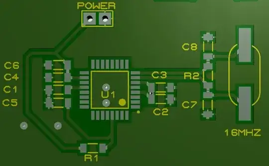
Is there an error in the basic schematic and PCB drawing of the Arduino?
-
That crystal might be a bit too far from the IC. But at only 16 MHz it might not be that big a deal. – Hearth Apr 16 '23 at 00:06
-
Yes there is. But it might not be very significant. – Justme Apr 16 '23 at 00:14
-
Should the crystal be closer to the avr than the resistor (R2) and capacitors (C7, C8)? – 571E Apr 16 '23 at 00:22
-
There are hidden pins on the schematic, or parts not shown. Crystal position is fine. Ground pour has almost no stitching. – Tim Williams Apr 16 '23 at 00:31
-
I’m on mobile so maybe it’s just me, but it doesn’t look like there’s a ground/Vdd connection on the mega – Bryan Apr 16 '23 at 00:31
-
I've read a lot of articles about components on pcb (especially capacitors between vcc and gnd), so I'm a bit confused. If this circuit design is a seamless circuit; I will use this in all my projects. That's why there are no other components in the schematic. Tim I added 2. pcb design, I think you recommend it to be like this. – 571E Apr 16 '23 at 00:53
-
Why there is a 1 megaohm resistor between crystal pins? Do you intend to work at 5V only or with lower supply voltages? Do you plan on doing timing critical stuff - if not the crystal is useless. If reset pin has a capacitor, you might want to add a diode too. Oh and you have no mechanism for uploading any programs, so the design can't do anything. – Justme Apr 16 '23 at 11:46
-
I apologize to all of you for the lack of information when opening the topic. Yes I did not specify spi port or any input-output pin, because I am trying to build the basic circuit. No privacy status :-). I'm removing the 1M resistor, it will only work with 5v, no critical timing condition, what diode should I add or remove the capacitor? – 571E Apr 16 '23 at 13:23
2 Answers
If you want to use the ADC, then add a little coil (10µH) from Vcc to AVcc and add bigger capacitors at every position too. I use 100nF and 4.7µF at Vcc and AVcc.
You need a ISP programming port to flash the bootloader or flash the device directly with the program.
There is no voltage regulator, you should add the possibility to add a 3.3V voltage regulator and use a crystal with 12MHz or lower if you want to use 3.3V sensors. The most external sensors what you can buy for arduino have voltage shift-transistors, but this is suboptimal. If you want to use a SD-card (3.3V), then it is better to connect it directly.
You can add some more vias under the chip for better GND connection.
You should put the capacitors as close as possible to the chip, may be under the chip (at the bottom side) so that the traces of the I/O-pins can go to the side and on a header or pad or to a sensor/actor.
- 1,338
- 2
- 11
-
1-Is it okay to add coils even if we don't use ADC? 2-Yes I did not specify spi port or any input-output pin, because I am trying to build the basic circuit 3-It will only work with 5v 4-I will add more vias near GND 5- Ok Thanks, Thanks for your warnings. – 571E Apr 16 '23 at 14:04
-
The ISP-Port (In System Programming - Port) is part of the minimal circuit. Some people remove the GND-area around the crystal so that there is no influence with the crystal. I normally let the GND-area there and sometimes connect GND with the shielding of the crystal. :-) – MikroPower Apr 16 '23 at 18:11
-
-
@571E - For the ADC, you can use a Electrolytic one, but I use SMD ceramic capacitors. They are only for filtering noise on the power rail. This is a simple LC-filter. – MikroPower Apr 17 '23 at 11:17
It seems you already have a power connection to C2 & C3 (via). If you moved R1 & C5 to the lower right of U1 you could connect their needed power trace on or near to C2, (instead of routing the long power trace loop along the left side). Eliminating that long trace would also eliminate the GND island connecting the grouped capacitors on the left.
On C2,C3, having a via directly connected to the SMT pads is not the best option. If the via connection is cooler it could act as a heat sink during the soldering process and possibly make a cold joint or mis-align the component. If the via is hotter is could wick solder away from the SMT pads. Having a small bit of solder mask and a short trace length between the via and the SMT pads will usually prevent soldering problems.
For better documentation take advantage of spare text attributes on components. For example you could add the physical pin connections to the text attribute on some of the bypass capacitors, (on the schematic a few have unknown positions). That will help during routing and even later on if any trouble shooting is needed.
If you are going to add multiple GND vias they may as well be placed where they are most useful. For example near component GND pins. For example the vias under U1 could be placed nearer to pins 2,5, and 21. Placing vias nearer to some of the bypass capacitors can reduce the loop length back to the GND pins, for example C1 & C3.
On the schematic C2 is shown on U1 pin 18, however the PCB has C4 is on pin 18, (same value so no operating issue, just a documentation issue).
- 7,939
- 15
- 19
-
Thanks for the warnings, I will try to re-edit it according to the information you have told. – 571E Apr 16 '23 at 14:07


