I have designed the circuit shown below for a reference current of approximately 1mA and an output current of approximately 100uA. I have observed that I am able to supply approximately 100uA to load resistances up to ~50kOhm. Afterwards, the output current starts to drop significantly. I assume this is because of the voltage drop at collector terminal of the Q2 transistor due to increase in load resistance.
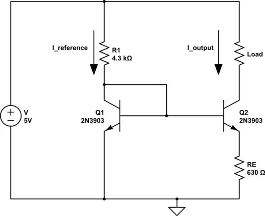
simulate this circuit – Schematic created using CircuitLab
I am trying to graph the output impedance of the current mirror versus the output current. I have calculated the output impedance of my circuit to be around 1.3MOhm (using Rout = ro[1+gm(RE//rpi)] ). I will assign parameter sweep to the degeneration resistance to vary the output current to see changes on output impedance. The load resistance will be kept constant at 1kOhm.
I can easily measure the output current but how can I measure the output impedance of my circuit in a simulator? I am using Tina-TI.
Edit: I obtained beta for Q2 as 70 regarding hfe/Ic curve in Onsemi datasheet for 2n3903. Va = 40.

