4

EDIT: I've redone the MOSFET circuit diagram; it now represents what my actual layout is. I wanted to spare myself redrawing the circuit but ended up confusing everything, I hope it's clearer now! Also, I'm using IR2907 MOSFETs, in case this is useful to anyone

I'm currently trying to build a half-bridge PWM speed controller for a 24 V, ~100 A, 2 hp brushed dc motor (circuit schematic is at the end; I made it using parts of other schematics found on the net) (circuit layout pictures also in the post).

It worked fine when controlling a small 12 V toy car motor.

When I tried hooking up my final layout (2 hp motor, 12 V lithium battery for the driver Vcc, two 12 V car batteries in series for the motor), it worked fine until the driver (IR2103(S)) started smoking, then sparked and finally caught on fire (cf. following picture showing blown up driver).

[It seems like the blowup is located at pin number 6, which is vs. too much current going in the driver from the motor?]

enter image description here

Something I've noticed when driving both the small and large motors, is that the motor speed reaches a maximum at around ~80% of the 100 kΩ potentiometer range, then falls off when I would've expected it to keep increasing. The oscilloscope reading of the 555 output showed 100% duty cycle but with a lot of instabilities and noise when going in that region.

When I tested with the large motor, the driver blew out when I reached that "fall-off" region and stayed there for a few seconds. I also wasn't using the large 10 µF capacitor across the 24 V battery and the RC snubber.

Here are my ideas of what caused the driver failure:

  • Lack of capacitor across the 24 V battery

  • Lack of RC snubber across the motor

  • 555 timer unstable beyond 80% of potentiometer range

  • Too much current going through the driver, causing it to fail due to overheating

  • Lack of MOSFET gate resistors?

Here are my questions:

  • Could you please help me identify what caused this driver failure?

  • Could you give me some advice to help me improve my driver circuit design (missing components, poor component choice, wires too long, parasitic inductance/capacitance, etc.)?

  • Could you help me understand and solve that 555 timer "fall-off" issue?

Here are the schematics of the circuit:

enter image description here

enter image description here

Here is a picture of the layout (without the motor and the batteries), with the MOSFET circuit on the right-hand side; I used aluminium strips for the large amperage (this will be cooled by a fan in the final build); I've also added a switch for the 24 V battery (in black); larger wires are the fours wires going to the MOSFET circuit (HO, LO, Vs and GND); smaller wires are Vcc, GND and the three potentiometer wires:

enter image description here

I thank you in advance for your time, knowledge and any advice you can give me, as drivers are quite expensive and I hate de-soldering components :)

Have a nice day!

ADDED:

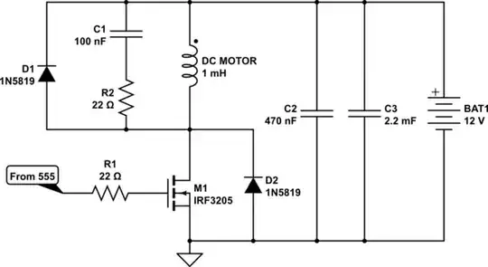
@EdinFifić Is this the circuit you suggest I should try?:

enter image description here

There are a few things I don't quite get:

  • Using a driver with a second MOSFET will give a lower voltage drop on the "off" part of the PWM cycle because instead of going through the body diode (in red), the back-emf current will go through a fully conducting MOSFET (which has a lower voltage drop)? Have I understood right?

  • What are the advantages to using a driver (and a second MOSFET) apart from the lower voltage drop then? Maybe it is more useful for smaller motors where voltage drops matter a lot more?

  • Shouldn't there be some kind of buffer between the 555 output and the MOSFET gate?

  • Should the grounds of both the 12 V Vcc battery and the main motor battery be connected?

  • If I choose to use a driver, which one would you recommend and/or which datasheet characteristics should I pay the most attention to?

Thank you again for your time

winny
  • 13,064
  • 6
  • 46
  • 63
Solmyr999
  • 67
  • 7
  • "Drive Mosfet" is reverse polarity. The other is correct. At least if you only look at drain and source. Otherwise strange orientation of the polarities. Deviating from norms and conventions leads to irritation and error. – arnisz Apr 14 '23 at 16:59
  • 1
    the battery symbol does not match the polarity labels in the schematic diagram ... the long bar is the positive end of the battery – jsotola Apr 14 '23 at 17:03
  • 2
    Thank you for choosing a mosfet driver with built in dead time, however be mindful that this configuration requires the duty cycle never hit 100% or the high side bootstrap supply will become discharged and the high side fet will not be fully enhanced. With typical layouts this would blow the high side fet, however your layout is different and may survive. – Bryan Apr 14 '23 at 20:12
  • I noticed the fet heatsinks getting slightly warm but I thought this might be normal for them to heat up. So, do you think the driver blowing up might be due to me wanting to reach 100% duty cycle ? – Solmyr999 Apr 15 '23 at 08:23
  • 1
    @Solmyr999 I am preparing my answer, took me a long time, will post it now, but I have more to add, so come back around to check it. I will let you know here when it's completed, but at least you will have most of the answer now. – Edin Fifić Apr 15 '23 at 08:41
  • @EdinFifić Thank you for your time! I've redone my MOSFET schematic because I screwed it the first time (please check my edit). It now represents my actual layout. – Solmyr999 Apr 15 '23 at 08:46
  • 2
    Please not that 100 % duty cycle will not be possible with a bootstrap. Actual limit depends on several things, but if you need above say 90 %, you need a dedicated floating supply for your high side MOSFET. Having your driver on a perf board with cable connections to your MOSFETs is simply not going to work. You need a dedicated PCB with strong ground plane and very short traces. – winny Apr 15 '23 at 11:26
  • The power side of your late addition schematic urgently needs a GND connection. (I'd find an additional polarity indication reassuring with "your batteries".) – greybeard Apr 16 '23 at 12:24

3 Answers3

4

Your first problem is your timing circuit.

enter image description here

DC motors are generally controlled with a low-frequency PWM drive of 25-100 Hz, about 400-500 Hz in some MCUs (like Arduino), and 1-2 kHz at the most. Your RC values indicate a 12.37 kHz frequency, which is too high for DC motors.
According to the formula in the below image, taken from Electronics Tutorials, your half-period at 50% setting (potentiometer in the middle) would be 40.4 us (micro-seconds), the total period 80.8 us, giving the frequency of about 12.37 kHz.
enter image description here

So, the first thing would be to greatly reduce the frequency by using at least a 10 nF timing capacitor (C1); I would recommend 100 nF.
The same site/page mentioned above has this schematic for PWM motor control:
enter image description here
As you can see, the R1 from your schematic is increased to 10 kΩ, and the timing capacitor to 100 nF. The same tutorial mentions the duty cycle range of 5-95%, so 0-100% is likely unattainable.

Your second problem with the increasing duty cycle comes from the IR2103 limitations on timing. You have indicated the motor speed dropping when you go above 80% duty cycle. That would be about 80 kΩ for the ON time, which would be about 0.8 x (80 kΩ x 1nF) = 64 us, which gives an OFF duty cycle of about a quarter of that, or 16 us.
According to its datasheet, first you have the "propagation delay" (the time it takes for the ON signal on its input to appear on its output, which could be as high as 0.8 us:
enter image description here
Then you have the "dead-time" (pause between turning one transistor OFF and the other one ON) of up to 0.65 us for one, 1.3 us for both combined.
This gives about 2us and if we add the 0.2 us turn-off propagation delay, it comes up to about 2.2 us in total delays of the IR2103.
Yet more delays to add to the above are the turn-on rise and turn-off fall times of about 0.2 us total at 1000 pF load (MOSFET input capacitance). Since your MOSFET is specified at 7500 pF (datasheet), these rise and fall times would be about that many times higher or up to about 1.5 us in total.
Not only that, the MOSFET itself has the turn-on delay and rise time of 0.16 us. Adding all these delays up gives you about 3.9 us, almost 4 us!

The third problem and finally the reason your IC burned out: your assumption about the pin 6 (VS) is correct.
The datasheet mentions the absolute maximum ratings for this pin: VB - 25 V to VB + 0.3 V.
The internal schematic shows details, but is not showing a Schottky diode which is likely placed between VS and VB (RED diode in the diagram) OR two output MOSFETs body diodes (BLUE on the diagram) which would explain the VB+0.3 V as its maximum potential:
enter image description here My thinking as to why it failed:

  • when the lower transistor switches off, the motor coil acts as an inductor which produces a powerful high voltage spike; the longer the duty cycle, the more accumulated energy in its magnetic field and the more powerful the spike - that's why it burns when you go above 80%;
  • the spike voltage adds up to the positive supply potential (if one end of the motor is wired directly to V+ supply line) and it can easily exceed the V+ + VB (almost +24 V in your case with 12 V supply, and almost +36 V with 24 V supply). This, combined with the fact that the boost potential VB is actually lower (possibly less than V+) when your duty cycle approaches 100%, and it becomes even easier for its current to go through the IC's output diode(s) on VS towards the VB pin;
  • if your motor is connected to the lower power supply rail (V- or 0V), then its negative voltage spike can be absorbed by your lower MOSFET's body diode, so it's harder to see how the IC fails in that case.

SOLUTIONS:

  1. Decrease the 555 frequency, in other words, increase the timing period by increasing R1 to 10 kΩ and C1 to 100 nF;
  2. Get rid of the IR2103, as you're not getting anything more from it than from the NE555 alone - both have about 200 mA current sourcing and sinking capability, so you're not improving anything by adding IR2103;
  3. Use a single MOSFET as a current sink for the motor, meaning connect one end of the motor to V+ supply rail and the other to the MOSFET's drain electrode. Now you should be able to go up to almost a 100% duty cycle (as much as the 555 can go);
  4. Definitely place an RC snubber across the motor, or even a diode;
  5. Place a 10 Ω resistor between the 555 output and the MOSFET gate to dampen ringing/oscillations.

ADDED ANSWERS (answering more questions afterwards is not practiced here, but I will just give short quick answers):

  1. Yes, you understood the MOSFET vs diode drop right.
  2. Advantages are lower energy loss, less waste heat and thus smaller components/heatsinks.
  3. 555 doesn't need buffer to drive a MOSFET at low frequencies (up to 10 kHz).
  4. The grounds should be connected for the MOSFET source to be at same ground as the 555.
  5. Almost any that suits your needs, too much to go over right now.

I have come up with a better schematic:

schematic

simulate this circuit – Schematic created using CircuitLab

This is just a rough idea, some values/components need to be changed, but it's a start.
Across the motor, you can use either a diode (D1) or the RC snubber to prevent high voltage spikes from destroying the MOSFET. The direction of the current from inductive kickback is the same as the current running the motor, which means its voltage adds up to the supply voltage (the dot end becomes negative and the opposite end positive).
D2 is the braking diode. As the DC motor continues spinning in the same direction after the power is disconnected, it starts generating current in the opposite direction, meaning its dot end is positive.
D2 in that case allows the current to flow from the dot end of the motor through the battery and back into the motor from the opposite end (conventional current flow), completing the circuit.
You should use a Schottky diode because it has a lower voltage drop than the MOSFET body diode (usually).
C2 and C3 are needed to absorb all the transients and peak currents: C2 would be a non-polarized, film capacitor of at least 470nF and up to 10uF and C3 would be at least 1000uF low-ESR type and should be a few of them in parallel to absorb such large currents (up to 100A).
A film capacitor could accompany each parallel electrolytic low-ESR capacitor.
You would also need to parallel a couple MOSFETS (while providing a larger current driver for all of them) and use at least AWG 4 (or 25mm²) copper wire...

There are quite a few caveats of circuit design involving large current/power, and it is not meant for a beginner. I have spent months searching for larger power solutions in couple specific cases because the current involved was over 40 amperes.
Anything over 10 A starts becoming a more serious business, growing exponentially (as the loss is squared with the current). It is the reason you will rarely see hobby kits running more than 10 A, because it needs more serious/hefty wiring/traces/circuits/boards/cooling, and things heat up and burn rather quickly.

Edin Fifić
  • 5,188
  • 7
  • 24
  • Thank you very much for your amazing answer ! When I was looking on the net for how to size my components, I found that tens of kHz PWM frequencies were fine for dc motors, but I guess I must have missed some important details. – Solmyr999 Apr 15 '23 at 08:56
  • When you talk about the driver timing limitations and delays, do you mean that the PWM frequency is too high and the driver doesn't have time to switch on and off properly ? (these are the kind of details I have a hard time understanding) How would the timing limitations cause the driver to blow up ? – Solmyr999 Apr 15 '23 at 08:59
  • 1
    @Solmyr999 The high frequency means shorter duty cycles, which means increased effect all the delays will have on the total circuit. I am preparing the last part of my answer, will let you know when I add it, which will explain why your IC burns out. – Edin Fifić Apr 15 '23 at 09:01
  • 1
    @Solmyr999 At 100Hz, a full cycle will be 10ms, so 10us delays will be only 0.1% of the switching (PWM) frequency, basically nothing. But at 10kHz, a full cycle is 0.1ms or 100us, which makes the 10us delays a full 10% of the cycle, which can significantly affect the circuit. Not only that, when you use a 20% cycle in that case, 10us is HALF of that cycle, and it gets worse as the cycle shortens. – Edin Fifić Apr 15 '23 at 09:08
  • Ok I understand now. When I think about it, driving such a heavy motor doesn't require a high PWM frequency at all. I should have delved deeper into this while designing my circuit ... but I guess this is good learning experience! – Solmyr999 Apr 15 '23 at 09:13
  • 1
    @Solmyr999 You actually learn more from such mistakes, and they leave a deeper and more lasting impression. You get to understand circuits and components at a deeper level. If you always had circuits that work without problems, you wouldn't know about the practical issues/problems in the real world. That's why those datasheets have so many details which look like too much at first, but when you start facing issues, those details can be lifesavers. – Edin Fifić Apr 15 '23 at 09:18
  • 1
    @Solmyr999 I have added more to my answer, should be complete now. Let me know how it goes for you. – Edin Fifić Apr 15 '23 at 12:07
  • Thank you very much for your complete answer ! That explains a lot and gives me many topics I need to look into more in details. Thank you for your solutions! – Solmyr999 Apr 15 '23 at 16:15
  • I have another question however : my idea by using a half bridge with two MOSFETs was to be able to use regenerative braking to recharge the battery (I want to use this setup on a bike). What you're suggesting is driving only one MOSFET directly from the 555 output, is that correct ? That will make regenerative braking impossible, right ? – Solmyr999 Apr 15 '23 at 16:17
  • 1
    @Solmyr999 The thing is, even without the upper MOSFET driver, you get regenerative braking because the upper MOSFET body diode will conduct. The only difference with the driver is you will get a lower voltage drop, from around maybe 1V down to less than 0.5V at 100A. What I'm saying is that it's not a huge difference, out of the maximum possible 2400W, you might lose up to about 50W which is not a relatively high loss. I missed the part about regenerative braking. In that case IR2103 can help, but there are integrated circuits which provide even more MOSFET driving current. – Edin Fifić Apr 16 '23 at 04:55
  • 1
    Thank you again for your answer! I've posted an answer to this post with a schematic of what (I think) you are suggesting. I also have some additional questions if you have some time. I am still in the middle of reading the Art of Electronics and more generally learning electronics, so there are many circuit design subtleties and hands-on experience that I don't have. – Solmyr999 Apr 16 '23 at 09:47
  • `if one end of the motor is wired directly to V+ supply line` is not what I see in both schematics, the motor having been left out of the picture. And if indeed the motor is driven in low side configuration, something is needed for Vs not to be driven way below GND. Given the low side MOSFET's body diode, its gate drive wouldn't make much of a difference but for recovery. Control of braking is minimal; regenerative braking won't happen without elaborately designing for it. – greybeard Apr 16 '23 at 11:51
  • 1
    @Solmyr999 - Hi, I note that you have chosen one of the least bad options and have moved your additional questions from a (non-)answer, into the question. (Therefore your comment above that you have posted an "answer" is now misleading, unfortunately.) Please note that you cannot keep adding questions *especially* after you have received answers. Your question is in danger of becoming (if not already) a "chameleon question" and may be closed or ignored as just too unclear / "moving goalposts" etc. || Remember that SE is not a forum - ideally a question *should* not change after being asked. – SamGibson Apr 16 '23 at 12:31
  • @Solmyr999 I also have the Art of Electronics. Great book for learning many techniques and subtleties of electronic circuits, but it requires a lot of time to read and digest. If you have more questions, I will try to answer them when I get a chance. You can post questions on StackExchange or we can move to private messaging. Comments are not for extended discussions. – Edin Fifić Apr 16 '23 at 16:48
  • Thank you a lot for all your answers, I really appreciate it ! I will keep delving into all this and follow your advices. I'll stop bothering you now! Have a nice day! – Solmyr999 Apr 16 '23 at 19:18
  • 1
    @Solmyr999 I have added more to the end of my answer. – Edin Fifić Apr 16 '23 at 20:08
  • 2
    One more very important thing is that one or more capacitors are needed across the 24 VDC supply, close to the MOSFETs. I would suggest a 1000 uF low ESR electrolytic, and a 470 nF film capacitor (polypropylene or polyester). Also, routing of grounds and power bus need to be carefully considered, with current approaching 100 A. – PStechPaul Apr 16 '23 at 22:09
  • 2
    @PStechPaul You're right, I completely forgot to add that, and it was a major thing I was going to suggest. A cold got me bad, it's hard to focus. I am adding them now. – Edin Fifić Apr 17 '23 at 01:20
1

Here's a major error in your design: -

enter image description here

The high-side drive and low-side drive don't match the polarities of the MOSFETs.

However, your hand-drawn schematic indicates you may have got this right?

enter image description here

But, the other side of the story is that you may have got your MOSFETs upside down: -

enter image description here

Anyway, something is screwed up in the diagram you posted. Any engineering saying: the devil is in the detail.

Working on breadboard is also going to throw up many problems.

Andy aka
  • 434,556
  • 28
  • 351
  • 777
  • 1
    Actually it's worse than that... check the battery polarity... or MOSFETs, or motor position! – Tim Williams Apr 14 '23 at 16:18
  • Please check my edit; I've redone the schematic to match my actual layout. I wanted to spare me the effort of drawing a schematic and ended up screwing everything... The hand drawn schematic is the right one – Solmyr999 Apr 15 '23 at 08:42
1

To anyone still wandering around here, I think I've finally found out why everything failed : when taking my circuit apart, I noticed that both mosfets were dead (gate-drain short on the low-side mosfet and gate-drain-source short for the high-side one). When searching for causes on the internet, I found that it's commonly caused by voltage transients and motor brushes noise and will often kill the driving circuits also (driver blew up and the 555 timer was later found dead as well).

So in the end : one 555, one mosfet driver and two power mosfets dead only because I didn't bother with transients and noise reduction when setting up my circuit for testing.

An (expensive) error I will remember.

Solmyr999
  • 67
  • 7