In the class AB amplifier shown below, we use diodes to make the PNP and NPN conduct equally.
How do the diodes make them conduct equally?
Is there some intuition I could use to understand this phenomenon?

In the class AB amplifier shown below, we use diodes to make the PNP and NPN conduct equally.
How do the diodes make them conduct equally?
Is there some intuition I could use to understand this phenomenon?
Voltage drop over one diode is approximately equal to voltage drop over Vbe.
So voltage over diode compensates for the drop caused by Vbe.
How does the diodes make them conduct equally? Is there some intuition I could understand this phenomena?
Instead of looking at a push-pull stage, it's equally relevant to see what happens when an NPN transistor is set as an emitter follower with no base-biasing (switch1 deactivated). This mimics the top half of the push-pull stage: -

With switch1 deactivated, the base of the transistor is not being biased. This is Class B operation. If you look at the load current in R1 (green), you can see that current flows for significantly less than one half cycle.
You could probably imagine the equivalent PNP emitter follower circuit that feeds load resistor R1; it would also conduct current over significantly less than the other half cycle: -

Now, if I throw the switch and allow a little bit of base biasing we get this picture: -

Note that I moved the \$V_{IN}\$ node marker (red trace) onto the base so that the bias voltage increase can be inspected.
Can you see that the transistor is conducting for about 50% of the waveform now? This is because the base-emitter region has been biased positively. And, if you imagine the PNP section was also present, you would see a fairly linear transition between NPN conducting and PNP conducting. This is Class AB operation.
But, why use a diode you might ask. The diode has a similar temperature characteristic to the base-emitter region and, if the diode is thermally linked with the transistor, as things warm up and the transistor base-emitter characteristic changes, the bias at the base would also do the same. So, the diode provides both biasing AND temperature compensation.
The diodes are used to provide the voltage needed to overcome the barrier to base current. This can also be done with resistors but diodes have the advantages of thermal compensation (if bonded to the power transistors thermally) and low ac resistance.
The diodes do not guarantee equal currents in the transistors. If the load is dc coupled to the emitters, then the equality of the currents depends upon parameter matching between the transistors.
The matching of the bias components will play a large role in current match.
The best way to intuitively explain a circuit idea (in this case "biasing") is to follow its evolution from the very beginning by building and exploring the circuit step by step.
I will do it here using CircuitLab in two ways:
I am happy that I finally managed to find a way to move the CircuitLab "parameters" window. The problem was that when I opened it to change the quantities, it covered the gauges and circuit elements, and I had to close it to read them.
You can trick it in this way:
So the idea is to dock the window and move the schematic.
Here is my story in seven parts...
Imagine we have a varying input voltage source Vin and we want to get an output voltage Vout that is "shifted" by a constant value. Our source is grounded and its initial voltage is 0 V; we can then change it via "parameters".

simulate this circuit – Schematic created using CircuitLab
We will sweep the input voltage from -10 to +10 V.

In some cases (e.g., when driving NPN transistors) we want to "lift" the voltage in the positive direction. KVL gives us an idea of how to do it - by series summing the voltages. To do this, we connect the "bias" voltage source Vbias1 ("battery") in series with the input source, with its negative terminal to it.

Thus the total voltage Vout follows Vin's variations with a constant offset (1 V in the schematic).

In other cases (e.g., when driving PNP transistors) we need to drop the voltage in the negative direction. Now we connect the bias "battery" Vbias2 with its positive terminal to Vin...
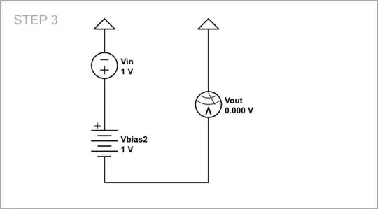
... so the total voltage Vout follows Vin's variations with a constant offset of -1 V.

In the OP's case (driving both NPN and PNP transistors), there is a need for two voltages "shifted" in opposite directions. So we have to "stick" the two configurations above connecting a positive "battery" Vbias1 with its negative terminal to Vin and negative "battery" Vbias2 with its positive terminal to Vin.
The two output voltages follow the input by being spaced with 2.Vout (2 V).

It is not convenient to use multiple "floating" voltage sources in circuits; instead, these voltages are taken from the power source. It is convenient for the purpose of biasing to use voltage drops across forward-biased diodes because the transistor inputs (base-emitter junctions) behave like diodes.
To put in practice this idea, we have to "stretch" (by two "pulling" resistors R1 and R2) the string of two diodes between the supply rails (to make a connection with the circuits above, I have used ideal diodes with VF = 1 V). We can liken this to a more sophisticated "tug of war" game where the players pull the rope with equal strength but we (Vin) come and grab it in the middle and start pulling it back and forth:-)
As you can see, the graphs are almost the same as above. They differ only at the ends where the input voltage approaches the supply rails and the voltage across the RD network significantly decreases. Then the current through the corresponding diode (D1 at +Vin and D2 at -Vin), respectively the voltage across it, decreases.

Finally we get to the real (OP's) part. We connect our biasing circuit to an imperfect emitter follower without biasing (aka "class B").
I have connected two perfect ammeters to measure the collector currents Ic1 and Ic2. Now about the load where I have used a little trick. To keep the circuit so symmetric and beautiful:-), I have used another ammeter both as an ammeter IL and... as a "load". For this purpose, I have worsen (increased to 100 ohm) its resistance in the parameters window; so you do not have to worry about it burning.
Let's first examine the circuit "statically" by applying three typical values of the input voltage. It is interesting to see what state the transistors are in and where the output currents flow.
DC input voltage source:
Vin = 0 V (grounded input). First we need to roughly adjust the bias voltages so that the transistors are slightly "open" and a small (say 2mA) initial ("quiscent") current flows. For this purpose, open ideal diode "parameters* windows and looking at ammeters, adjust their VFs so that Ic = 2 mA and IL or VL = 0. It is not very easy; it takes some skill and patience... and a willingness to do it (to some it would seem pointless). Thus Q1 and Q2 act as emitter followers and can be thought as some "voltage divider" stretched between the supply rails.
Vin = 5 V: Only Q1 act as an NPN follower; Q2 is off. Significant 50 mA current flows through Q1 and the load RL that form a "voltage divider".
Vin = -5 V: In this case, only Q2 act as a PNP follower. The same 50 mA current flows through RL and Q1 in the oposite direction. Now they form a "voltage divider".
So, figuratively speaking, we can think of Q1, Q2 and RL as some 3-resistor "voltage divider" in a "star connection". Two of them (Q1 and Q2) are dynamic and the third (RL) is constant.
AC input voltage source:
Let us now examine the circuit in the classic way by applying an AC input voltage. Vin is a functional generator with DC offset voltage; so you can also apply a DC voltage as above.
Vin = 100 mV: First, I suggest that it be of small amplitude (100 mV) in order to observe well the "shifted" base voltages.

Vin = 9.5 V: If we significantly increase Vin close to the supply voltage, we will see how the output voltage "saturates" because the input base voltages stop changing.

Experiments with biasing:
Vbias1 = 0 V; Vbias2 = 0 V (no biasing): We see that in the region from -0.7 V to 0.7 V there is no output voltage because both transistors are off.

Vbias1 = 400mV; Vbias2 = 400mV: At a small bias voltage, this region narrows and distortions decrease...

Vbias1 = 583.66 mV; Vbias2 = 655.3 mV: ... and at normal bias voltage, the distortions completely disappear.

In this way, we can precisely adjust the bias voltages to obtain a perfect output signal.
Conceptual circuit. The problem of the simple diode biasing is that the current through diodes depends on the input voltage. The reason for this is that the "pulling" resistors are constant when the voltage varies. A neat trick is to make them "dynamic" so that the V/R ratio (current) stays constant. This means that when Vin increases, R1 decreases and R2 increases, and vice versa. Such nonlinear resistors can be modelled in CircuitLab by current sources.
As we can see from the graphs of the bias voltages, now they do not "saturate".

Practical circuit. In real amplifier circuits, the output (collector-emitter) parts of transistors can act as such "dynamic resistors".
Finally, we can draw an interesting conclusion about this network of four elements in series: They are all "dynamic resistors" - diodes are "constant-voltage" and transistors are "constant-current" elements. So when the current tries to decrease, the diodes increase and transistors decrease their "resistances". As a result, the voltage drops across diodes an the current through them do not change.
First, understand why the crossover distortion happens in the first place.
The transistors are being used as common-emitter follower drivers, arranged as a symmetrical push-pull pair.
You may remember that an NPN common-emitter follower voltage output is offset by one base-emitter drop (Vbe) below the input, about -0.7V. Likewise, a PNP follower will have its output one Vbe above its input, about +0.7V.
For the single class-A follower this Vbe-to-output offset isn't usually a problem. However, connecting together a pair of complementary followers as a push-pull class-B, and you get crossover dead-band: while the input is in between +Vbe and -Vbe, both transistors are off and the output undriven. This is the cause of the distortion.
We can compensate for the Vbe drop and get rid of the dead-band by pre-biasing the bases with a compensating offset: +Vbe for the NPN, -Vbe for the PNP.
As it so happens, a silicon diode has about the same forward drop (0.7V) as a transistor base-emitter junction. We use a pair of diodes together with resistors to create two offset base drive signals, in each case 'lifting' (pre-biasing) transistor bases into near-conduction.
Here's an uncompensated class-B push-pull side-by-side with an improved, pre-biased one (simulate it here):

The reduced distortion is evident in the right-hand (improved) circuit (hint: add 'spectrum view' to the scope plot to see the difference in harmonics.) Note: what's being shown is a DC-coupled amplifier. You can insert a capacitor to make it AC- coupled. Regardless, the base drives are 2x Vbe (about 1.4V) offset from each other.
The 'base lift' pre-biasing diode approach used here is effective, if not precise. Nonetheless it’s pretty good at eliminating the bulk of the dead-band to create a lower distortion class-B amplifier. This circuit can be further improved upon by adding some form of negative feedback, and also by modifying the transistor biases into class-AB type operation (that is, include some idle current.)
Speaking of which, want even lower distortion from your push-pull output? The Blomley amplifier is a highly-regarded approach that uses both offset drives and has idle bias current, among other improvements. Read on.
Or, try it (simulate it here):
