4

Consider the following almost-surely-wrong comparator circuit:

schematic

simulate this circuit – Schematic created using CircuitLab

In various places I've seen similar circuits, some have R3, some have R4, some have neither. Similarly, some have R5, some have R6. (Some have neither, but those are "without hysteresis" and can be ignored. AFAIK, none have both. Here, an absent resistor should be removed entirely along with its connections.)

What is the purpose of R3/R4 and how does one know when they can be omitted? How does one know whether to include R5 or R6?

Matthew
  • 481
  • 2
  • 12

4 Answers4

4

Typically, you either want hysteresis (caused by positive feedback) or linearity (achieved with negative feedback).

Linearity will be important for amplifiers, such as audio applications. In such cases, you employ negative feedback:

schematic

simulate this circuit – Schematic created using CircuitLab

In all these configurations above, inverting and non-inverting, some fraction of the output potential is fed back to the inverting input, so that feedback is negative. They all produce an output highly proportional to the input, one of the great benefits of negative feedback in general.

I won't go further into detail about why R4 is or isn't necessary above, since you can read about that in any op-amp literature about linear amplifiers such as those. I will simply say that R5 in your own circuit is necessary if you require linearity, and R4 will almost always be present, which in combination with R5 sets the fraction of the output fed back, to determine "gain". R5 can be zero, in which case you have a "voltage follower".

Mixing both positive and negative feedback creates a situation in which one will dominate, completely nullifying any effect of the other. Having said that, it is possible to employ resistors R5 and R6, if you require a linear function of two separate input potentials, but it's too complex a topic for here. If positive feedback is dominant (your goal is to implement hysteresis), there's no reason that I can think of to also have negative feedback.

Your question suggests confusion mainly about resistor use in positive feedback configurations. Positive feedback causes the output to slam hard against one of the power rails, forming a digital "high" or "low" state, and it's impossible to get such systems to settle in the middle somewhere.

This is great for switching applications that require clear on/off signalling. Positive feedback results in hysteresis, very desirable for noise immunity, and perfect for preventing oscillation. Positive feedback, as you have guessed requires a feedback resistor (R6 in your circuit, and mine below) to cause a shift in potential at the non-inverting input.

Let me restate that with emphasis: hysteresis requires positive feedback, so R6 is always required, but the presence of R6 must result in a shift of potential at the non-inverting input as the output swings between high and low.

If the potential at the non-inverting input is held fixed by some voltage source, no amount of feedback via R6 can possibly influence that potential! Consider the following two circuits:

schematic

simulate this circuit

Note: R1 in these circuits, and the ones below, is the pull-up resistor necessary for many "open collector output" comparators, such as the LM393. Not all comparators require it.

Clearly both of these produce a low output when IN is above 5.1V, and high otherwise. On the left I provide a reference potential at the non-inverting input using a voltage source, and on the right I use a zener diode for the same purpose.

You might expect R6 to provide some hysteresis, but in both cases R6 is useless. That's because the reference potentials are very low impedance voltage sources, and no amount of pulling up or down of that potential by R6 can have any effect. Well, the zener diode reference isn't quite as "stiff" as the voltage source, and so there might be a little wobble of potential, but this is far from ideal.

In such cases where the potential at the non-inverting input is "held steady" like this, you need to provide a little flexibility there. That's the role of R3:

schematic

simulate this circuit

Here R3 is used to increase the reference source impedance, so that it can actually be "tweaked", or modulated by output transitions. R6 now has a fighting chance to actually influence the potential at the non-inverting input.

The amount of influence that the output has on the non-inverting input potential (the feedback), will correlate with the ratio between R6 and R3. The lower R3 is, the "stiffer" the opposition to change. The lower R6 is, the "stronger" the output can pull up or down.

R3 won't be strictly necessary if the impedance of the source providing the potential at the non-inverting input is already high. For instance, you may wish to use a resistor potential divider to present, say, a third of the supply potential, which I do here with Rx and Ry:

schematic

simulate this circuit

I can dispense with R3 here because the two resistors in the divider already provide a potential at their junction with quite a high source impedance. That potential is therefore already very "flexible", easily influenced by feedback via R6.

That source impedance (and its consequent "flexibility") becomes quite obvious when I replace the system consisting of Rx, Ry and the supply (in the blue box), with their Thevenin equivalent circuit, shown above right. Those two circuits would behave identically.


Update

To have the output go high when \$V_{IN}\$ exceeds some reference, IN must drive the non-inverting input, and now you must consider the impedance of the source of potential at IN. The only difference between the following two designs is the presence/absence of R3:

schematic

simulate this circuit

These two circuits are presented with an input, the blue trace below, a potential sweeping up from 0V to 8V, and then back to 0V. The left circuit's output is orange, and the tan trace is from the circuit on the right:

enter image description here

Hysteresis is only present for the left circuit (orange), and can be seen as two distinct switching thresholds at the green markers. Due to the zero impedance source V1, I've had to include R3 to permit R6 to modulate a little above, and a little below the potential at IN, prior to presenting that potential to the comparator's non-inverting input.

The tan plot (from the right-hand circuit) shows not even the slightest trace of hysteresis, because without R3, there's nothing that R6 can do to fight against the might of source V1.

Simon Fitch
  • 27,759
  • 2
  • 16
  • 87
  • BTW, did you notice your schematics are all inverted compared to what's in the question? You have Vin going to '-' and Vref going to '+'. That means you're throwing resistors at Vref, whereas my application needs resistors on Vin. I'm fairly confident I understand how things need to get switched around, but just saying... – Matthew Apr 12 '23 at 21:39
  • Op-amps and comparators usually have the inverting input (-) on the top and non-inverting (+) on the bottom. – PStechPaul Apr 12 '23 at 23:06
  • @Matthew For the comparators I wanted to illustrate the conditions under which R3 is necessary, at the *non-inverting input*. It doesn't matter whether that input is driven by a reference voltage \$V_{REF}\$ or some signal being measured \$V_{IN}\$, if the source is low impedance then R3 is necessary. – Simon Fitch Apr 13 '23 at 04:28
  • @PStechPaul, blame CircuitLab. Point is, my example was outputting Vin > Vref; these are all outputting Vref > Vin. – Matthew Apr 13 '23 at 14:12
  • @Matthew, I've updated the last example with inverting and non-inverting inputs swapped, to get you a high output when Vin > Vref. – Simon Fitch Apr 13 '23 at 15:08
1

R1 and R2 provide a reference of 1/2 V1, or 2.5 VDC.

R5 and R4 comprise negative feedback for gain, but that is not really useful in this case, so R5 would be omitted and R4 could be replaced with a short, so the inverting input oculd be connected directly to the 2.5 V reference point. But it is good practice to use a resistor for R4, with a value close to the combined resistance of R6 and R5, that compensates for bias current.

R6 provides positive feedback to the non-inverting input, so when the voltage of the sine wave signal exceeds about 2.5 V, the output will go positive, which adds to the voltage on the non-inverting input and causes a sharp transition with hysteresis. The amount of hysteresis will be determined by the ratio of R6 and R5, where R6 is usually much larger than R5.

(edit) Following simulation with bias current R5=R6=10k. And R8 should be labeled R3, and R9 should be R6, and R7 should be R5, to match OP's circuit.

schematic

simulate this circuit – Schematic created using CircuitLab

Voltages with R9=3k, R8=R4=1k, R7=50k Linear slope transition

Simulation

Voltages with R8=1, R4=1k, R7=50k Sharp transition with positive feedback (hysteresis), but no bias compensation shows unequal on/off output

Simulation

Voltages with R8=R4=1k, R7=50k With bias current compensation, shows equal on/off output

Simulation

PStechPaul
  • 7,195
  • 1
  • 7
  • 23
  • Uh... I think you've mixed up some identifiers. I have **never** seen a circuit with both R5 and R6. [This calculator](https://www.daycounter.com/Calculators/Comparator-Hysteresis-Calculator.phtml), for example, omits R4 and R5, and cites R6/R3 as the important ratio. (Identifiers are according to the circuit I gave in the question, not as they appear in the calculator.) If I set things up as you indicate, CL is very unhappy, wants possibly-infinite time to run the simulation, and the result is clearly not as intended. – Matthew Apr 12 '23 at 14:58
  • Also, can you please clarify the purpose of R4? It doesn't seem to affect the simulation. You say it "compensates for bias current"; what does that mean? – Matthew Apr 12 '23 at 14:59
  • A "real world" comparator or op-amp will draw some current on the inputs. This will change the voltage from that which is expected, because the external circuitry will have a finite impedance. So, for instance, if CMP1 has a bias current of 1 uA, it will cause Vref to be pulled down by 1 uA * 100 ohms = 100 uV, to 2.4999 V. In your example with R3=100 ohms, R4 is not needed and may be detrimental. But if R3=1k and R6=10k, R4 needs to be about 1k to match impedances and maintain an accurate switching threshold. – PStechPaul Apr 12 '23 at 19:47
  • Thanks, that helps. Don't R1/R2 factor into that, though? Say I have R1/R2 = 3k/1k giving me 3V from 12V. R3 = 3k, R6 = 150k. (Tₕ ≈ 3.06, Tₗ ≈ 2.82.) If I couldn't care less if those values are "wrong" by ±0.1V, is there any point to R4? (They are at least wrong by the same amount, I think?) ...p.s. I'm still fairly confident your answer is wrong; I think you meant R3 and R6 everywhere you paired R5 and R6? Also, your answer as written seems to recommend 150k for R4 as described in this comment, while your comment seems to suggest R4 ≈ R3? – Matthew Apr 12 '23 at 20:15
  • You might be right, but the principles I show in my circuit are correct. The default op-amp in CircuitLab has non-inverting (+) input on the bottom. You have used a comparator, which may be labeled differently. – PStechPaul Apr 13 '23 at 21:49
1

I'm going to attempt to answer this on my own, based mainly on looking at this calculator and fiddling with simulating that configuration:

schematic

simulate this circuit – Schematic created using CircuitLab

First off, it helps to understand the basics, namely, that the comparator outputs a 'high' voltage when its '+' input is higher voltage than its '-'. I believe the output voltage depends on the specific comparator, and, particularly, what supply voltage (VCC) is provided. (The CircuitLab simulation appears to use a fixed 5V.)

Knowing that, what's going on with R6? Well, when the comparator output is 'low', a small amount of current wants to bypass the comparator and go directly to M1. The result is that the voltage the comparator sees on it's '+' is slightly lower than Vin. In this example, the R1/R2 voltage divider is providing 2.5V, so the comparator will switch when Vref is slightly higher than that. (Simulation and/or the previously linked calculator can provide more precise values.)

Once that threshold voltage is exceeded, however, and the comparator output switches to 'high', the current flow through R6 will switch directions and start to "back-feed" the comparator's '+'. This causes the voltage seen on '+' to jump slightly. As a result, when Vin starts to fall, the comparator won't switch back to 'low' until Vin falls "significantly" below Vref. This is important because it prevents rapid switching due to noise from Vin. Essentially what we've done is create a range of voltage such that the comparator only switches 'high' when the upper threshold is crossed, and only switches 'low' when the lower threshold is crossed. Any fluctuation whose magnitude is less than the window size won't cause a transition.

The exact values of "slightly" and "significantly" are determined by the ratio of R6 to R3, where R6 is typically much larger (often by at least an order of magnitude) than R3. Again, consult a calculator for more precise values. Of course, it should go without saying that R3 is always necessary.

What about R5? Well... having the back-flow on '-' instead of '+' means that, when Vref and Vin are similar, as soon as the comparator switches, Vref gets "tweaked" in a way that reverses the comparison. For carefully tuned values, this can "stretch" the transition from a sharp on/off into a bounded linear mapping from input to output... but we're discussing digital comparator logic, not linear amplifiers. For poorly chosen values, it will result in the comparator switching as rapidly as it can when given a particular range of inputs. While there are applications for the former, and might be some applications for the latter, this is absolutely not the way to build a Boolean-logic voltage comparator.

For how to rework this to output 'high' when Vin is less than Vref, see Simon's extremely detailed answer.

(Astute observers will notice I didn't mention R4. Something mutter something "bias current" and "read about that in any op-amp literature about linear amplifiers". Honestly, I'm lost there.)

Matthew
  • 481
  • 2
  • 12
  • The core idea of hysteresis is: net positive feedback. As long as it is achieved, what resistors are present doesn’t matter. All the resistors shown in the circuit in the question can be present if the application calls for it. To figure out their allowed ranges takes some algebra. – Kuba hasn't forgotten Monica Apr 12 '23 at 17:55
  • @Kubahasn'tforgottenMonica, hmm, possibly, but in what cases would you actually *want* R5? It would, at least, have to have higher resistance than R6, and it's unclear what purpose it would serve. – Matthew Apr 12 '23 at 18:04
  • Remarkable reasoning... I read your answer to your own question with the great pleasure I feel whenever I see a thinking person... I would be happy to join this discussion (especially regarding when and why R5 is needed)... but I need some time to catch my breath because I just finished a long answer. (@Kuba hasn't forgotten Monica, sorry for the intrusion) – Circuit fantasist Apr 12 '23 at 19:36
  • My expanded answer shows what happens when negative feedback is provided via R5. There may be some combinations of negative and positive feedback that result in instability. – PStechPaul Apr 12 '23 at 22:55
1

The inertia of verbal clichés

As in life, we name circuit phenomena with specific names, terms. Such are, for example positive feedback, hysteresis, negative resistance, differential resistance, etc. There is nothing wrong with this because it creates convenience in communication. The bad thing is when these terms wear out of use to such an extent that we forget what is behind them and use them mechanically. And the worst is when we use them to explain circuits to beginners without revealing their essence.

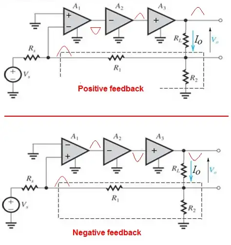
Hysteresis and positive feedback

It is generally accepted that the two phenomena are equated... but I dare say that they are different. Indeed, in electronic circuits, hysteresis is often implemented using positive feedback, but this is not mandatory; there can be hysteresis and no positive feedback. An example of this is the famous timer 555.

What hysteresis is

It means that when the input voltage rises the comparator switches at a higher threshold than when it falls. We can do it in two ways:

With two thresholds implemented by separate comparators

In this arrangement there is no positive feedback from the output to the input (the output voltage is not added to the input voltage). There is only positive feedback in the RS latch but this is another story. An example of this configuration is the timer 555.

With a changing threshold implemented by one comparator

The idea is that after switching at the upper level, the output of the comparator will "help" the input source and thus make the threshold lower. This can be done in two ways:

  • by adding voltage to the input voltage of the non-inverting input

  • by decreasing the voltage of the non-inverting input.

The comparator does it during the transition with the help of the positive feedback.

What positive feedback is

This is positive feedback "out of control" or as they call it, "self-reinforcing positive feedback". Note that there is positive feedback for an extremely short time, only during the transition. The rest of the time, the comparator output voltage has reached the supply voltage and there is no gain.

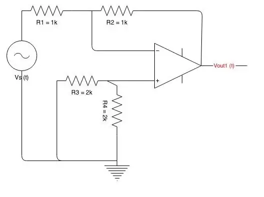
Positive and negative feedback

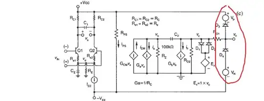
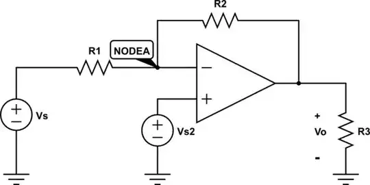
The time has come to reveal the role of this mysterious resistor R5 in the OP's schematic...

The idea. Some electronic circuits (I have considered four notable solutions below) inherently have positive feedback, but we want them to operate in linear mode (steady) like amplifiers. So we apply the following trick - we add negative feedback so that it dominates over the positive one and eventually the circuit works with negative feedback.

Implementation. In the conceptual schematic below, both feedbacks are implemented by voltage dividers. For the circuit to be stable, the negative feedback voltage (on the inverting input) must be higher than the positive feedback voltage (on the non-inverting input). This is usually provided by the input elements being connected to the non-inverting input.

schematic

simulate this circuit – Schematic created using CircuitLab

As we can see, the resistor R3 (the OP's R5) is a part of the negative feedback network. So it is not necessary for the OP's comparator with hysteresis that needs only positive feedback. Regardless, since the OP is interested in this topic, I will consider a few famous versions of this configuration below. Some of them are even named after their inventors. I will reveal the idea of ​​each of them in several successive steps accompanied by CircuitLab simulations.

"Negative resistor" (INIC)

This simple circuit with the complex name "current inversion negative impedance converter" (INIC) consisting of an op-amp and two or three resistors is the basis of the following circuits. Its idea is very simple and intuitive even though it is not explained like that in textbooks. Let's follow it...

Positive load: If we connect a voltage source with Vin = 1 V to a 1 k "positive" load RL, a current IL = 1 mA will flow from the source to the load. Thus, the source "produces" and the load consumes energy. Figuratively speaking, RL acts as a "pull-down" resistor.

schematic

simulate this circuit

Negative load. Now, if we connect RL as a "pull-up" resistor to twice the voltage 2.Vin (obtained by an amplifier OA with a gain of 2), the same 1 mA current will flow through it but in the opposite direction - from the load to the input source. The current has reversed its direction from RL to Vin and this creates the illusion that the load has become a source and the input source has become a load.

schematic

simulate this circuit

Note that the network of 2.VL source and RL in series "produce" a current that is proportional to the voltage VL, i.e., it acts as a resistor but with a "negative resistance" -RL.

Implementation: Above I made the op-amp gain 2x by setting it in the CircuitLab parameters window. In real circuits, we do this through the principle of negative feedback, forcing a huge gain op-amp to only gain 2x by a simple trick - connecting a voltage divider with an inverse "gain" of 1/2 between the output and its inverting input. Simply put, this is how we made a non-inverting amplifier with a gain of 2.

schematic

simulate this circuit

The only difference with an ordinary non-inverting amplifier is that here there is also a resistor between the op-amp output and the non-inverting input... and this gives the circuit the "magic" properties of behaving like a "negative resistor".

Load canceller

Once we have created a negative resistance, we can use it to destroy an equal value positive resistance. The result in this circuit (INIC) is infinite resistance (by the way, there is a dual circuit VNIC, in which the result is zero resistance). Let's thus, in three steps, destroy the harmful 1 k load connected to a relatively high resistance 10k potentiometer.

Potentiometer unloaded: I have supplied the pot by +10 V voltage source and set the wiper in the middle (K = 0.5 in the P parameters window). So the voltmeter shows exactly 1/2 of the voltage.

schematic

simulate this circuit

Now let's see, by the help of DC sweep simulation the graph of the output voltage when the wiper "moves" from the one to the other end (K varies from 0 to 1). The graph is absolutely linear.

Potentiometer unloaded

Potentiometer loaded: If we connect a relatively heavy 1 k load, Vout drops to 1.4 V...

schematic

simulate this circuit

... and the graph is very nonlinear.

Potentiometer loaded

Potentiometer compensated: But we connect our magic negative -1 k resistor in parallel with the "positive" 1 k resistor, and the miracle happens. The voltage across the load is the same as if the load is not there...

schematic

simulate this circuit

... and the output voltage graph is just as linear as when there is no load.

Potentiometer compensated

The explanation is simple - now the "negative resistor" (and not the potentiometer) supplies 1 mA current to the load RL. The potentiometer does not "see" a load but open circuit.

Howland current source

The idea of ​​this and the next circuit is to maintain a constant current through the load by adding a "helping" current to the initial one, i.e. they are ways of making a constant current source. Let's build the first.

Perfect current source: An "ideal" current source keeps the current through the load constant even as the load changes its resistance. Here I have used a little trick to simplify the schematic - I have set 1 k resistance of the ammeter. Thus it has become a "load".

schematic

simulate this circuit

We see that even if RL varies, the current remains constant.

Perfect current source

Imperfect current source: But when we try to make a 1 mA current source by connecting a 1 V voltage source and a 1 k resistor in series, the load causes problems with its resistance and the current drops in half.

schematic

simulate this circuit

Imperfect current source

Perfect Howland current source: Howland's idea was to connect a "negative resistor" in parallel to "help" the load. Now, when RL increases, the initial current Iin decreases but the "helping" current coming from the op-amp output through R1 increases.

schematic

simulate this circuit

So their sum IL through the load does not change.

Howland current source

Deboo integrator

I dedicate this part of my answer to Gordon Deboo, the inventor of this famous circuit, with whom I had the good fortune to correspond years ago. Some time ago, I came across a link to the correspondence uploaded by him on Google Sites. There, he has told how he invented this and other remarkable circuit solutions.

As we can see from the link above, Deboo came up with this idea independently of Howland and used it to make a non-inverting integrator (especially valuable today in single-supplied op-amp circuits). We follow a similar building scenario.

Perfect C integrator: If we supply a capacitor by an "ideal" current source, we obtain a perfect integrator...

schematic

simulate this circuit

... with linear curve through time (use time-domain simulation).

Perfect C integrator

Imperfect RC integrator: When we make a simple resistor current source, the voltage across the capacitor is subtracted from the input voltage and the current decreases.

schematic

simulate this circuit

The curve is nonlinear (exponent).

Imperfect RC integrator

Perfect Deboo integrator: Deboo had connected a "negative resistor" in parallel to help the imperfect input current source. As a result, the current through the capacitor was constant...

schematic

simulate this circuit

... and the curve was linear...

Perfect Deboo integrator

Circuit fantasist
  • 13,593
  • 1
  • 17
  • 48
  • 1
    Probably TMI for the OP's needs, but a very carefully detailed explanation and presentation of various useful circuit implementations. Plus one... – PStechPaul Apr 13 '23 at 22:29