0

There is a constant leakage current flowing through the detector (SiPM) shown in the circuit below. It causes a constant shift of the baseline in the output of the voltage amplifier. Is there a way to make the output baseline adjustable or very close to zero?

Edit:

  • I am not interested in the DC component in the signal.
  • The op-amp is powered by a single USB connection for convenience.
  • A SiPM is an array of multiple avalanche photodiodes. At room temperature avalanche will happen in ~10 kHz even without any light. This creates a constant reverse leakage current through the device. When the device is hit by many photons at the same time, a current pulse larger than the dark current will appear. C5 is used to supply charges needed to maintain that short-lived large current pulse.
  • The final goal is a transimpedance amplifier that picks up sudden current changes from the detector (SiPM) and outputs it as a voltage signal with a baseline at zero. If there is a better solution than the one shown below, that is acceptable too.
  • I am aware of charge-sensitive pre-amps. But I am afraid of the constant pulse piling up at their outputs due to the existence of dark pulses from a SiPM.

enter image description here

Jing
  • 157
  • 7
  • Is DC part of your bandwidth of interest? Your amplifier is amplifying DC, is that intended? – Designalog Apr 11 '23 at 05:58
  • I can see that you are using the op amp in single supply config, so the output can be up to 0.3V for zero input. What level of shifts are you talking about? – Rohat Kılıç Apr 11 '23 at 09:13
  • 2
    If DC is not of interest, how about blocking it using a DC blocking capacitor? – sai Apr 11 '23 at 12:06
  • @RohatKılıç, you’re right. Could you please explain the origin of the 0.3 V shift? The shift I saw is a few times larger. But I’d like to get rid of the shift from the single supply configuration as well. – Jing Apr 11 '23 at 12:07
  • @ErnestoG, no, I don’t need any DC component from the diode. Is there a way to block the DC component? – Jing Apr 11 '23 at 12:09
  • That 0.3V shift comes from the op amp's design. See the datasheet, find the output swing spec. Typical 0.1V but can be as high 0.3V. This means that the lowest output you can get from that is 0.1~0.3V higher than the negative supply (ground - 0V, in your case). You can't get rid of that shift. – Rohat Kılıç Apr 11 '23 at 12:47
  • @sai, where shall I place the capacitor? I thought about replacing R1 with a capacitor, but the right side of the capacitor has no current source. You can only charge it from the left side. Isn't that a problem? – Jing Apr 11 '23 at 13:16
  • @Jing, how much voltage do you measure on the +ve terminal of the opamp and how much on the output of the opamp? – sai Apr 11 '23 at 13:40
  • It's most likely that the photon multiplier has a reverse leakage current that is more significant than other leakages. Please link the device. – Andy aka Apr 11 '23 at 14:06
  • @Jing the way you have wired your amplifier will amplify DC as well. Put a high pass filter at the input and a capacitor in series with R6. – Designalog Apr 11 '23 at 16:01
  • @ErnestoG, the resistor in a high pass filter will provide a way to charge the capacitor from the right side. That would solve the problem I mentioned 4 comments above. I guess its value should be much smaller than R5 to allow AC current to pick that route. The bandwidth of the op-amp is 100 MHz. If I use a 10 nF capacitor, my resistor would be at 2pi Ohm to keep that bandwdith. Does that make sense? – Jing Apr 11 '23 at 17:54
  • @ErnestoG, what's the usage of a capacitor in series with R6? – Jing Apr 11 '23 at 17:57
  • @Jing it'll become an open at DC, thus your amplifier will be a buffet at DC, preventing it from amplifying its own DC offset. – Designalog Apr 11 '23 at 18:14
  • @Jing beware of the high pass resistor noise. If you make it smaller, you might make its input referred noise voltage very large (yes, larger makes its noise referred to the input smaller) – Designalog Apr 11 '23 at 18:15
  • 1
    @ErnestoG, would you like to put everything together in an answer? – Jing Apr 11 '23 at 18:32
  • @sai, the voltage at the output is about 2.6 V. the -vee is connected to the ground on the PCB I am testing. – Jing Apr 11 '23 at 19:36

2 Answers2

1

I'm no expert in SiPM, but based on quick read at this article (https://www.onsemi.com/pub/Collateral/AND9782-D.PDF), it appears that if you take the input signal from the "fast output" pin of the SiPM, then this signal is effectively AC coupled.

For now I'm going to ignore that and just focus on your schematic as it appears.

First, we need AC coupling to prevent the (+) input of the amplifier from sensing DC. A resistor to ground then follows in order to form a high-pass filter and bias your input to some voltage. If your supplies were bipolar, then you could simply connect the resistor to ground. However, your supplies appear to be unipolar; therefore, you need to connect that resistor to some middle voltage, perhaps 2.5V might be a good idea.

Second, any op-amp has an equivalent voltage offset referred to its input. You can ignore everything from your input signal and just consider how this DC signal will be amplified towards the output by a factor of 11 (the non-inverting gain of your op-amp). To avoid this, you need to make the equivalent impedance of R6 infinite at DC. This can be achieved by simply adding a capacitor in series with it to ground. It'll also define, partly, your -3dB frequency as a high-pass.

There are also other considerations. The value of this high-pass resistor must be large. Why? Assuming the 100nF is a short at your frequencies of interest, then your SiPM is effectively connected to AC ground. However, your SiPM has a parallel capacitive impedance.

If you refer the current noise of this high-pass filter resistor to the input (I'm assuming you have replaced R1 by a coupling capacitor). Then you'll effectively have a voltage noise due to the coupling capacitor (which can probably be ignored at your frequencies of interest), and another voltage noise due to R5.

How do I know this? You can use the Blakesley shift theorem (a very old theorem that is criminally ignored by most mainstream texts, unfortunately). You can check this answer I wrote where I show how to use this theorem to calculate input-referred noise effortlessly. Hopefully, then you'll be able to follow what I'm saying above.

Here's also a GIF I came up with to show how to use this Blakesley shift theorem without much text. It's not exactly your schematic, but I think it'll help you quite a lot:

Blakesley Shift Theorem

This noise voltage due to R5 I mentioned earlier is basically amplified towards the output by your 1 + R3/R6. You could argue that is somewhat low-pass filtered due to the capacitive impedance of your SiPM to ground, but I'm guessing this is happening at very high frequencies that you won't be saved by it at your frequencies of interest.

Designalog
  • 3,232
  • 1
  • 13
  • 23
1

This offset that you are trying to eliminate might actually be a good thing, because no op-amp is really capable of producing an output potential equal to its lower supply, even so called "rail-to-rail" devices, or ones that explicitly claim to produce outputs right down to the lower supply.

If you use a single-ended supply, with the op-amp's lower supply at 0V, a more realistic lower limit to the output might be +50mV. Your attempt to remove the offset, to obtain a quiescent output of exactly 0V (in the "dark"), amounts to asking the op-amp to produce an output of 0V, which it simply cannot do.

The output, then, of your op-amp has a lower constraint, but so does the input. Many op-amps will not behave well when either of their inputs falls below the lower supply potential. Some (older models) will even send their output right up to the maximum possible, a phenomenon called "phase inversion".

This is why in most tutorials and documentation, the op-amp usually has a negative supply too, to avoid these inconveniences. Ironically, in your circuit, the slight positive offset at the input that you are trying to eliminate might be the only reason the thing works at all.

If you did have a negative supply for your op-amp (even if only slightly negative), then the output and input ranges can include 0V, and removal of the DC offset component is trivial. Simply decouple the feedback path from ground, with capacitor C6 here:

schematic

simulate this circuit – Schematic created using CircuitLab

It will take a few milliseconds following power-on for the output to settle to 0V, while C6 charges up to the input signal's mean potential. Like all AC coupled stages, if input potential remains higher than baseline for an extended period, this AC coupling capacitor will charge over time to the new mean, and when the input returns to its usual level, the op-amp output will be momentarily negative. And vice versa.

If you don't have a negative supply, then I'm sure you don't want to have to add one, and you're not alone. But the sad truth is that no op-amp can output a potential very close to its negative supply, and this has consequences for any stages that follow, including any analogue-to-digital converter (ADC).

No subsequent stage should expect to receive a zero potential signal, and if that stage happens to be an ADC, then you have to accept the reality that this ADC input will never see less than +50mV (well, maybe less, but that depends on the op-amp model). In other words, you must expect to lose some of the lower counts of the ADC's full conversion range. If the following stage is another amplifier, then you must deal with the fact that the incoming signal will never be zero.

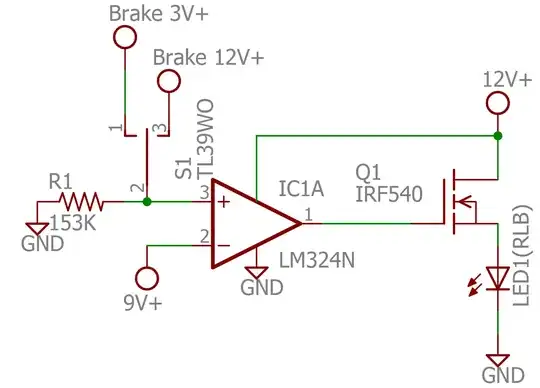
So, you don't have a negative supply, and you don't want to make or add one. All is not lost. You can create a new "supply rail" somewhere between the the ones you already have. One at, say, +0.1V. Then you may use this new voltage source as your "surrogate ground" for all the analogue stuff. If all analogue potentials are considered relative to this +0.1V, then it's as if you now have op-amp supplies of +4.9V and -0.1V. The op-amps don't care what you call "analogue ground".

There's one major requirement for this new "analogue ground"; that it be low impedance, low enough to stay fixed at +0.1V despite any load that may be connected to it. Here's one way to achieve that:
schematic

simulate this circuit

With negative feedback, the output of an op-amp is very close to zero, and will resist very strongly all attempts to shift it. However, most op-amps can only sink or source at most 10mA or so at their output, so we must still take care not to ask for more than that.

This "analogue ground" AGND can be used by any and all subsequent stages as a common point of reference, such that any signal with this potential is considered to be zero.

Now let's rebuild the above AC coupled, offset-cancelling amplifier, employing this new analogue ground:
schematic

simulate this circuit

I have told op-amp OA1, your amplifier, that the new reference baseline is AGND at +100mV. I have removed C6, and moved AC coupling to the input, a task now performed by C7 and R12. This ensures that quiescent output potential is also +100mV.

All op-amps following this stage can share this same baseline, and since none of them are being asked to produce 0V output, everybody's happy. If there's an ADC at the end of the chain, it too will see a baseline of +100mV, and you will have to compensate for this in software. Here I add a second gain stage, and give both stages a gain of 48, for a combined gain of 2300, and yet the output still has a quiescent potential of 100mV:
schematic

simulate this circuit

Simon Fitch
  • 27,759
  • 2
  • 16
  • 87
  • I love this place. People provide answers from different angles. @simon-fitch, thank you for pointing out that the output may be dramatically distorted when the input is very close to one of the limits of the power supply. I totally agree with you and realize that zero baseline and 0-5V USB power supply cannot work together. I am digesting your solutions. I don't understand why adding C6 can help zero Vout in your first circuit. When everything is stabilized, Vout = Vin- = Vin+ != 0. Am I missing something here? Could you please also explain why C1 is needed in your second circuit? – Jing Apr 30 '23 at 01:18
  • How easy is it to create a negative potential out of a 5V USB connection? Is it easier than providing the 100mV AGND? – Jing Apr 30 '23 at 01:20
  • 1
    @Jing C6 won't "zero" the output, it charges up with a DC level equal to the *average* of the input, which sets the average DC potential of both inverting and non-inverting inputs to be equal. That sets the output to have this same average too. I should have been more clear, this won't "zero" the output, it only means that the gain of 11 applies only to the AC part of the signal only, so while you still have an output offset, it is equal \$1\times\$ the input average, not \$11\times\$. – Simon Fitch Apr 30 '23 at 11:06
  • @Jing There are "voltage converter" ICs like the [ICL7660](https://www.renesas.com/us/en/document/dst/icl7660-datasheet) that can produce a negative rail from a single positive one using only a couple of extra capacitors. Don't forget that if your op-amps now have a negative supply, then they can produce outputs that can harm an ADC. This was my main motivation for suggesting a "mid-way" rail, rather than a negative one. – Simon Fitch Apr 30 '23 at 11:13
  • @Jing C1 is just filtering out some of the noise invariably present on the +5V rail. – Simon Fitch Apr 30 '23 at 11:16
  • could you please provide a reference that a negative input may harm an ADC? – Jing May 02 '23 at 20:25
  • @Jing Any ADC datasheet. For example, [ADS1115](https://www.ti.com/lit/ds/symlink/ads1115.pdf), page 6, section 7.1, "Absolute Maximum Ratings". Inputs are clamped by internal ESD protection diodes. An op-amp can easily source the 10mA clamp current necessary to cause damage. – Simon Fitch May 03 '23 at 00:12
  • Interesting. All ADCs I used so far accept both positive and negative signals. When a pulse is above or below the input voltage range, it is simply cut on the tip. Nothing bad happens to the ADC. A sound card also accepts both polarities. I was not aware of ADCs that only accept positive signals. – Jing May 03 '23 at 01:00
  • thanks for the detailed explanation of the usage of C6. Would you like to update your answer accordingly? Not everybody reads comments. – Jing May 03 '23 at 01:01