Understanding by explaining
There is a very interesting paradox in life that can be observed here very often: By asking interesting and unexpected questions, such curious young people make us think and rethink what we know about circuit phenomena. Thus explaining them, we understand these ideas even better... and continue explaining them:-)
How we should not teach
I first encountered this strange creation of human thought as a student in the late 1970s. Then TTL circuits were in their heyday and entire computers were made with them. I have kept the (unpleasant) memory of a laboratory exercise in Digital Circuits where the assistant made us do an experiment that was incomprehensible to me - to measure and plot the TTL transfer curve Vout = f(Rin)... not Vout = f(Vin) as I expected. It was indeed a virtuoso experiment, but not for a person seeing a TTL gate for the first time. I was tempted to reproduce it now (already with pleasure) after more than 40 years (see below).
Logic gate evolution
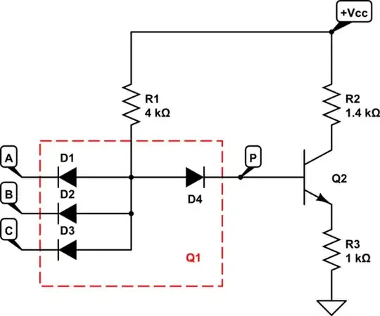
TTL gates are the successor of DTL gates; so the best way to explain TTL is through DTL as @G36 did in their answer. The common thing in both families is that the input logic variables control electronic switches - diodes in DTL, and transistors in TTL.
But there is a significant difference in the way the transistor Q2 is controlled - in diode circuits it is done by interrupting the base current, while in transistor circuits by shorting the base voltage. This allows Q2 to quickly turn off.
Operation
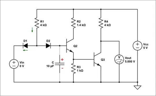
Let's consider the two implementations in parallel so we can compare them. For the purpose of understanding one input is sufficient (ie. we will explore the elementary logic NOT gate).
Vin = 0 V
DTL. When the input voltage is zero, D1 diverts the R1 current through itself; both D2 and Q2 are cut off (the current is "steered" to D1). The problem is that there is no return path for discharging the charge accumulated in the base, the charged stray capacitance C, leakages, etc.
simulate this circuit – Schematic created using CircuitLab
Let's now see the transfer characteristic Vout = f(Vin) by the help of DC sweep simulation. As you can see, I have set the input voltage Vin to vary from 0 to 5 V.
Improved DTL. So I would add an ideal diode D3 (with 100 mV forward voltage) in parallel to the network of two back-to-back diodes D1 and D2 to mimic the turned on transistor in the TTL gate below.
simulate this circuit
The transfer characteristic Vout = f(Vin) is almost the same as above; there is only a small shift to right that should be explained...
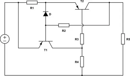
TTL. Here, the Q1 base-emitter junction corresponds to D1 and the base-collector junction to D2. Since the Q1 emitter is grounded and its base is connected through R1 to Vcc, Q1 is turned on and can sink a collector current. So the capacitor C will be quickly discharged through the Q1 collector-emitter part and the Q2 base will be firmly grounded.
simulate this circuit
Mimicked "charged capacitor". Since I don't know how the initial conditions of the capacitor can be set in CircuitLab, I have imitated it with the "pull-up" resistor Rtest.
simulate this circuit
Vin = 5 V
DTL. Now D1 is backward-biased and the R1 current is steered to right through D2 and Q2 base-emitter junction. So the Q2 collector current is increased enough and Vout is almost zero.
simulate this circuit
TTL. Now Q1 works in a very strange "inverse active mode" because everything is upside down - the emitter is "pulled up" to 5V, the base is "lifted" to the middle, and the collector is at its lowest voltage. Indeed, Q1 works like a transistor but we don't want that because its emitter consumes some (although small) current from the previous stage. I had a great desire to observe this phenomenon, but apparently CircuitLab gets confused and gives wrong values of the currents in the input circuit (you can check it to convince yourself).
simulate this circuit
Let's now see the transfer characteristic Vout = f(Vin) as above (the input voltage Vin varies from 0 to 5 V)...
... and the input characteristic Iin=f(Vin).
Mimicked inverse active mode. So to see it anyway, I decided to do the following trick - I "reversed" the transistor, with the collector out to 5V (as it works in "normal active mode") and reduced its beta a lot (below 1). So I was able to observe something close to my expectations.
simulate this circuit
The transfer characteristic Vout = f(Vin) is almost the same as above; there is only a very small shift to left...
... but the input characteristic Iin=f(Vin) is quite different.
My weird experiment of 70s
"Input resistor". Finally, I decided to reproduce the incomprehensible (to me) experiment from my student years. I used the DC sweep simulation by setting the resistance of the "input resistor" Rin to vary from 1.5 k to 2 k.
simulate this circuit
As you can see, the output voltage changes from 5 to 0 V as if there was an input voltage changing from 0 to 5 V like above. This is because the R1 current IR1 "creates" a voltage drop Vin = Rin.IR1 that gradually increases when Rin increases. You can also consider the two resistor (R1 and Rin) in series as a voltage divider with varying transfer ratio.
"Input load". Now we know that many circuits (e.g. microcontrollers) with built-in "pull-up" resistors at the inputs have this strange behavior - they pass current out and can power input devices. If I could go back 40 years now, I would have my young assistant (now retired professor) drive and simultaneously indicate the TTL inputs with low current LEDs :-)
simulate this circuit


