How to understand electronic amplifiers
It is a well-known fact that more complex electronic circuits can be explained and understood through simpler equivalent electrical circuits. Typically, controllable current and voltage sources are used to model the behavior of active devices. But they are abstract models that give only a formal idea and work well in circuit theory.
For the purpose of intuitive (true) understanding of circuits we need to go down to an even lower level and that is the concept of "controllable" and "dynamic" resistors. It is underestimated only for the simple reason that "resistance" usually means "linear" ("ohmic") resistance and transistors have non-linear resistance. For purposes of intuitive understanding, however, this is not essential.
That is why, I have explained below the idea of the complementary (push-pull) amplifier stage using only the concepts of variable resistor (rheostat), voltage divider and potentiometer. They are sufficient to build a functional idea of these circuit solutions. To show the relationship between the resistor and transistor circuit, I have considered them in parallel from the start to finish.
The push-pull stage is bipolar (split) supplied; so there is no need for coupling capacitors. This simplifies things and does not distract us with unnecessary details.
How to explore amplifier stages
I have used CircuitLab to simulate the circuits as follows. To keep the schematics simple, I have not used potentiometers as variable resistors but constant resistors with an arrow in pale gray. You can change their resistance by opening the parameters window and setting values in the field. If the window covers the instruments or labeled nodes, you can pull them out (along with the connecting wires) temporarily while setting values and then put them back. Also, you can make cloned instruments and labeled nodes.
The initial schematics look a bit oddly drawn because the idea is to complete them step by step. They are bordered in pale gray to appear at the same scale.
The parameters are adjusted to obtain the same values of voltage drops and currents in individual frames. The idea of this is to show that resistor and transistor circuits are equivalent. Resistance values are exemplary; I have chosen 1 k to be simple to calculate.
Building a simple amplifier stage
In fact, there is no amplification in the literal sense of the word; there is only regulation (reduction) of the power supply voltage.
Producing a positive voltage...
The first thing that comes to our mind to reduce the voltage is to connect a variable resistor R1 in series with the power supply and to change its resistance.
... by unloaded rheostat... But if there is no load connected, current does not flow, there is no drop and nothing changes - the output voltage remains equal to the supply voltage (I have chosen 10 V for simplicity). This goes against human intuition and it is good to experiment - open the R1 parameters and set different values of the resistance.
simulate this circuit – Schematic created using CircuitLab
... and NPN emitter follower unloaded. In a real amplifier (emitter follower here), an NPN transistor plays the role of R1. So open Vin parameters and set various input voltages. As you can see, the emitter output voltage does not follow Vin and stays equal to 10 V as above. So, we conclude, a transistor alone is not enough to make a follower... something else is needed...
... by loaded rheostat... That thing is the load RL. Let's load the rheostat R1 first. Now a load current IL begins flowing, a voltage drop VR1 = IL.R1 appears across R1... and we can change the output voltage Vout across the load within wide limits by varying R1. We conclude that R1 and RL form a voltage divider; so to change the voltage, we need two resistors forming a voltage divider.
simulate this circuit
... and NPN emitter follower loaded. Let's now load the transistor and begin changing the input voltage. Since there is a negative feedback, the transistor adjusts its "static" collector-emitter resistance Rce (corresponding to R1 above) so that to make Vout = Vin; hence the name "follower". As you can see, I have adjusted Vin to 5.701 V to obtain exactly 5 V at the output. Thus the Q1's collector-emitter "static resistance" is exactly Vce/IL = 5/5 = 1 k as the R1 resistance above. The transistor can only source current ("push" the load).
simulate this circuit
Producing a negative voltage...
All the configurations above are supplied by a positive voltage source V+; so the output voltage is also positive. If we need a negative output voltage, we should supply the voltage divider by a negative voltage V-.
... by unloaded rheostat... Vout is constantly -10 V.

simulate this circuit
... and PNP emitter follower unloaded. Also here.
... by loaded rheostat... Now we can change Vout. R2 and RL form another voltage divider.
simulate this circuit
... and PNP emitter follower loaded. Here the transistor follows the negative input voltage. It can only sink current ("pull" the load).
simulate this circuit
Building a "push-pull" amplifier stage
With the two types of configurations we assembled above, we can amplify either a positive or negative input voltage. In order to be able to amplify both, we obviously need to "stick" two complementary configurations together.
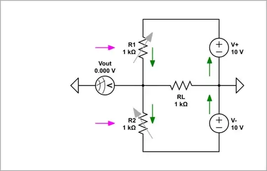
Differential voltage divider
Thus we get another (third) voltage divider composed of two complementary resistors R1 and R2 with oppositely varying resistances. Here again we need a bit more dexterity to change R1 and R2 "simultaneously" and oppositely while looking at the output voltage across the load.
simulate this circuit
In these differentially changing R1 and R2 we can see the ubiquitous potentiometer.
Potentiometer
simulate this circuit
It is interesting to see how the load impacts the potentiometer. Here is the result of a DC sweep simulation with three load resistances - 100 ohm, 1 k and 100 k. As you can see, the 100 ohm load is too heavy for the 1 k potentiometer. Figuratively speaking, there are three resistors "pulling" the common output point - R1 "pulls" it up, R2 "pulls" it down and RL "pulls" it to the middle point... and the first two must be stronger than the third.
Push-pull stage
Now it remains only to replace the resistors with transistors and we get the famous push-pull stage. The NPN follower will act during the positive input half wave and the PNP follower will act during the negative half wave.
simulate this circuit
But the problem with the unwanted Vbe voltage of the transistor appears.
0.7 V > Vin > -0.7 V. Actually, when the input voltage "wiggles" between -0.7 V and 0.7 V, both transistors are off... and we can remove them from the schematic.
simulate this circuit
Vin > 0.7 V. When Vin increases enough, the output voltage begins following the positive input voltage less by 0.7 V.
simulate this circuit
Vin < -0.7 V. Also, when Vin decreases enough, the output voltage begins following the negative input voltage more by 0.7 V.
simulate this circuit
Graphically presented.
Improving the "push-pull" amplifier stage
Biasing
The remedy is obvious - we have to apply a tiny initial voltage (about 0.7 V) across each base-emitter junction. This means to add this voltage to the input voltage and apply the sum to Q1's base, and to subtract it from the input voltage and apply the difference to Q2's base. We can implement it by two diodes (D1 and D2) connected in series. They are forward-biased through the "pull-up" resistor R1 and "pull-down" R2.
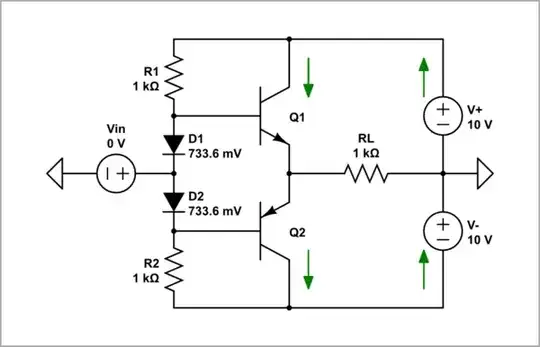
simulate this circuit
As you can see, the output voltage strictly follows the input voltage.
Overloading
But if the load is too heavy, another problem appears - at some value of the input voltage the output stops changing. Let's drastically reduce the load resistance (from 1 k to just 10 ohm) to observe this effect. It is convinient to use the DC live simulation - hover the mouse over the circuit components to find the reason. Aha... we see that the Q1's base current and accordingly, the voltage drop across R1, have significantly increased.
simulate this circuit
Straightforward solution
We can simply decrease the R1 and R2 resistances, for example, to 100 ohm...
simulate this circuit
... and the problem is solved. But now the current through diodes is very high (100 mA).
Elegant solution
We finally realize what the problem is - R1 and R2 are constant ("static") resistors. So, when Vin increases, the voltage drop across and the current through R1 decrease... and at some point the diode D1 turns off. The same happens at negative voltage with D2. So, the remedy is to make R1 and R2 "dynamic" - they have to decrease their resistance when the voltage across them decreases and v.v. In other words, they have to be "current-stabilizing resistors" (transistors).
Let's mimic their behavior using CircuitLab by manually changing their resistance as the input voltage changes. Here you will need even more agility than before because you will have to change three quantities at once - Vin, R1 and R2. For example, below I set Vin = 6 V; then decreased R1 by 500 ohm and increased R2 by 500 ohm. Thus, the total resistance R1 + R2 = 2 k remained the same and the current did not change accordingly.
simulate this circuit
Formal presentation
These "magic dynamic elements" are formally presented as "current sources".
simulate this circuit


