While this stacked arrangement of bipolar transistors is often taught to be an implementation of AND, it's fraught with problems, not the least of which is reverse-biased base-emitter junctions.
Base-emitter junctions behave like zener diodes, with reverse breakdown voltages as low as 5V. That junction begins to conduct when the base tries to drop lower than 5V below the emitter, and clamps the difference at 5V. In your circuit, if you raise the second input potential, the result is a current path shown in red here:
simulate this circuit – Schematic created using CircuitLab
That may or may not be problematic, but it's certainly not desired behaviour.
Another issue you face is what happens when you take inputs above 12V:
simulate this circuit
The base-collector junction is just another diode, conducting freely when that junction is forward biased. Here you see significant current flowing the wrong way through the load, which may not be enough to activate a relay, but it's not ideal.
Another problem is the stacking of collector-emitter voltage drops when they are all on. \$V_{CE}\$ can be many tenths of a volt (depending on the transistor model), when passing a lot of collector current. They all add up, reducing the voltage available for the load:
simulate this circuit
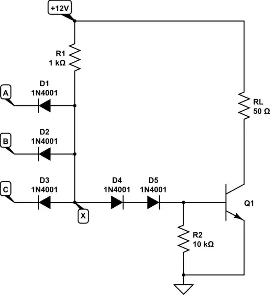
All these problems are easy to resolve. Here we use diodes D1, D2 and D3, and resistor R1, in a "Diode-AND" arrangement:
simulate this circuit
Node X is held high by R1, unless any of the inputs A, B or C are brought low. Then one or more of the diodes become forward biased, pulling X low. The forward voltage of those diodes prevent X from falling below the transistor's own base threshold, so we use D4 and D5 to raise the voltage required at X to switch on the transistor.
In your circuit, and mine above, we rely on the the gain of a single transistor to drive the load, but even with a gain of 100 or so, it requires significant current (tens of milliamps) from the inputs. Your 1kΩ input resistors dissipate more than 500mW, and would have to be quite beefy. These inconveniences can be mitigated with an additional transistor:
simulate this circuit
R1 has increased ten-fold, requiring input sources to sink only a milliamp or two. Q1 will sink about 10mA from Q2's base, and Q2 will be able to provide up to 1A to its load, if ever you needed that. Everything is much less stressed. The only other significant change is that the load is now low-side.
In both these last two designs, inputs can be 24V without upsetting anything, but anything above 0.7V will be considered "high".

