9

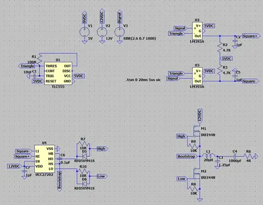
I am building a class D amplifer and I have getting shoot-through despite my best efforts to mitigate them using dead-time, miller clamping, and using high V_GS_threshold MOSFETs. Here is the circuit on LTspice:

Figure 1

The problem occurs when the high side switches on. You can see in the image below that the current through M1 and M2 spikes up. Building the circuit works but only if V2 is under 7 V and a PC audio volume less than 40%. If I increase either variable, the current spikes, activating my power supply's overcurrent protection and sometimes burning the UCC27282 MOSFET driver (I've burnt over 20 MOSFET drivers already, each costing me 4 CAD).

Figure 2

I initally thought I would need external dead-time, which I can add by adding two reverse parallel diodes on the inverting input of the comparator U3, thereby reducing Square-'s duty cycle:

Figure 3

Now going into the simulation, the shoot-through current is even worst, going from about 5 A previously, to about 27 A.

Figure 4

So, I undid the changes to the comparator U3 and decided I would test what would happen if I replaced the Square- signal on the MOSFET driver's LI with ground (I think doing this might affect the bootstrap circuit as the bootstrap capacitor is now charging through a higher impedance path via the load) and this is what I get.

Figure 5

WOW! 40 A of shoot-through current?! How is the low-side MOSFET turning on even though its gate voltage is zero? Or... is it? Upon further inspection there appears to be spike of 1 V of V_GS before completely going to zero. But the 1 V spike occurs when the shoot-through current drops and 1 V is less than the IRFZ44N's V_GS_threshold of 2 V. Is this actually not shoot-through current? Does the MOSFET enter the linear region? How am I in engineering?

If I replace the 10 kΩ resistors on the MOSFET's gate to source with 1 kΩ, there is a slight decrease in shoot-through current, it's almost negligible. I ended up reading about miller clamp circuits and thought that its low ON impedance would quickly discharge the MOSFET's gate-source capacitance as opposed to using a resistor. Still negligible effects.

I ended up trying a higher V_GS_threshold MOSFET (IRF530) instead, and the shoot-through current did decrease to about 1 A, but adding dead-time is still not completely getting rid of it.

Could someone please help me figure out this mysterious shoot-through problem (assuming it is even shoot-through) and finally put me out of my misery?


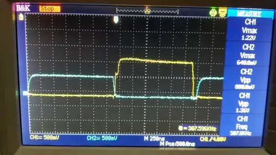
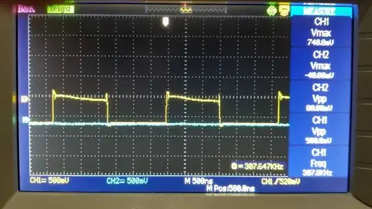
Here is the working circuit on a real scope. x10 attenuation is used to minimise probe capacitance. You can find the board layout link in one of the comments below (sorry, not enough reputation apparently).

In the image below, we have yellow as High (M1's V_G to GND), and blue as Low (M2's V_GS).

Figure 6

The yellow signal in the image below shows M1's V_DS, so my thinking here is that, M1 is ON when the V_DS is zero as that is the voltage drop across it.

Figure 7

Finally we have M2's V_DS as a yellow signal again. I can't have both V_DS show on the scope, since their reference points are not the same and I don't have differential probes. Yes, this is probably going to limit the information we have. Anyways, M2's V_DS looks weird since the wave is slanted a bit.

Figure 8


UPDATE 2023/03/25:

I made a new circuit board for the MOSFET driver and I discovered that using a different brand of capacitors for C7 (noise decoupling capacitor) fixed the slanted voltage curves from above. Below is an image M2's V_DS

Figure 9

You will notice that I'm using a higher supply voltage compared to the image above. That's because the current draw has decreased dramatically. Before, my circuit wouldn't even function above 7 V as the current would start rising exponentially over time. Now this circuit at 12 V is running only 27 mA without sound playing.

I've also tried out Simon Fitch's Miller clamping circuit on the actual circuit this time and here are the results. Blue is High (M1's V_G to GND), and yellow is Low (M2's V_GS).

Before enter image description here After enter image description here

You can see that the signal to M2 turns off a little faster and reduced the ringing on the High signal after it switches on. These results were taken after I replaced C7. I would also like to mention that before C7 replaced the ringing was much higher that it was outputing a constant high pitched noise on my speaker.


Conclusion So the issue in the live circuit was a bad brand of capacitors that were used for the MOSFET driver's noise bypass. I found out they were Tantalum capacitors and I believe all Tantalum capacitors are polarised and Ceramic capacitors are non-polarised. I blame the electronics shop for putting them in the non-polarised section.

My circuit now works as intented and even works in FULL-BRIDGE mode.

I am still not sure why LTspice is showing shoot-through. Even using Simon's miller clamp circuit didn't do much on the simuluations, but his answer proved to be useful in supressing ringing and quickening turn off times

I didn't end up trying Russel's snubber circuit as an extra 10 Ω would cause a huge voltage drop, reducing my output volume. However, I think his method is worth a try in combination with Simon's miller clamp circuit if anyone decides to use very low V_GS_threshold MOSFETs for their projects. I think in the live circuit, the MOSFET's V_GS while OFF is not reaching the V_GS_threshold, so there are no false turn ON's caused by it. Instead, it was the due to a wrong capacitor type that was adding a lot of noise into the MOSFET driver which caused the false turn ON's or semi-turn ONs as you saw in the M2's V_DS figure, where the voltage was slanted.

I would like to thank everyone for contributing their ideas. I know it's kind of lame that I'm solving my own problem, so I do apologise. However, Simon and RusselH provided a solution that improved the overall performance of my live circuit, which helped supress some of the noise from my speaker. The question regarding the shoot-though in the LTspice simulation is still up for grabs as I'm still very confused what is happening there.
  • 1
    Welcome! _”I've burnt over 20 MOSFET drivers already”_ Please show layout and oscillograms. – winny Mar 19 '23 at 21:03
  • It looks like the shoot-through spike occurs when the bootstrap voltage exceeds 12V, at which point the bootstrap capacitor starts charging. Also, is it possible that the inductive load is generating a voltage spike? It may help to add a 10 ohm or so resistor from the middle of the half-bridge to the bootstrap of the driver. The https://www.ti.com/lit/ds/symlink/ucc27282.pdf? has cross-conduction lockout, and your high/low signals don't seem to overlap. – PStechPaul Mar 19 '23 at 21:36
  • You don't show a bypass/energy storage capacitor on the 12V rail of the half-bridge, although that might not make a difference for this simulation. To truly replicate your circuit, the simulation should show small inductors and resistors on the power carrying connections. Also, your last image shows high current during a slow transition of gate voltage, where at least the high side would be in linear region. But it doesn't explain why the low side is also conducting, even with apparently zero gate voltage. – PStechPaul Mar 19 '23 at 22:18
  • Hey Winny, this is the link to my layout. https://oshwlab.com/electric_evan/class-d-amp-workshop. Please keep in mind that the layout states a 12 V open collector which is different from the 5 V in LTspice. I tried both voltages actually during testing. I'll also update the post to show real scope testing. Hi PStechPaul, a 10 Ω resistor between net bootstrap and the half-bridge middle didn't work unfortunately. Also, the capacitor you mentioned, would that be C7 (1 μF) on U4? (Should I put these as separate comments?) – Random Burnout Mar 19 '23 at 22:55
  • The fact that increasing the dead time increases the shoot-through suggests that perhaps your drivers are inverted and they are actually both on when you think they are both off? – user253751 Mar 20 '23 at 01:09
  • I would work in the simulator first since it does seem to be simulating whatever your problem is, and it saves you from replacing dead parts. Plot Id and Vgs for each MOSFET; do they look reasonable? In particular, Vgs isn't high for both at the same time.... yet somehow Id is? – user253751 Mar 20 '23 at 01:14
  • Are you making it on a breadboard? At 300 kHz, you are doomed to fail without a PCB with ground plane. – winny Mar 22 '23 at 10:11
  • Hey Winny, I actually got it working on breadboard as well! I do have to use a lot of filtering capacitor though, especially after a resistor. Although I'm not sure how add noise. – Random Burnout Mar 25 '23 at 19:42
  • @user253751: Or he didn't change the timing at all. That comparator has input current in the nano-amps, which will produce only a trivial forward voltage in the added diodes. – Ben Voigt Mar 25 '23 at 19:43
  • Hey Ben and user253751, U3's inputs are inverted to U2. So U3's output is inverted to U2's output. I did this since the LM393 comes with 2 comparators in an 8-DIP package and buying a dedicated inverter chip would just increase cost. The diodes are adding dead-time. I did not show the before and afters of Square+ and Square- here, but the simulations do show added dead-time. – Random Burnout Mar 25 '23 at 20:27

3 Answers3

11

I think it's Miller capacitance giving you grief. I think that the single-diode implementation of the miller clamp, that you have used (see below) is not working as you expect:

schematic

simulate this circuit – Schematic created using CircuitLab

V1 and V2 are ideal sources, producing the following potentials:

enter image description here

I've removed all capacitance from the transistor models, \$C_{ISS}\$, \$C_{OSS}\$ and \$C_{RSS}\$, and inserted a single capacitance C1 to mimic Miller capacitance. Obviously, this is an exaggerated scenario, but it's just to illustrate why the solution I propose at the end can work.

Without a clamp diode, Miller current causes a large voltage drop across R2, switching M2 back on momentarily. M1's drain current looks like this:

enter image description here

When we insert the diode, remembering that the source is ideal, Miller current is effectively bypassed, so only a volt or so appears across R2, and M2 stays off. Drain current stays low:

enter image description here

The diode does well, but its effectiveness depends on the source impedance of the driver. Since all that miller current is being fed right back into the driver's output, any impedance there will cause gate potential to rise, also. The diode is only bypassing R2, not the driver's own output impedance. Here I use R4 to mimic a source impedance of just a few ohm. Miller current through it will cause M2's gate potential to rise again:

schematic

simulate this circuit

Below is the resulting gate potential, where you can clearly see that it's enough to switch M2 back on momentarily. After that, the drain current spike returns:

enter image description here enter image description here

I suggest you try to divert Miller current direct to ground, with a PNP bipolar transistor:

schematic

simulate this circuit

In this way only 1% or so of Miller current makes it back through R2 and the driver's output impedance, and the rise in gate potential is attenuated, hopefully enough to prevent M2 from switching on again. Drain current is suitably dampened to a reasonable amount:

enter image description here enter image description here

winny
  • 13,064
  • 6
  • 46
  • 63
Simon Fitch
  • 27,759
  • 2
  • 16
  • 87
  • 1
    I agree with Simon. If your layout is genuinely on a breadboard as per the link, or something similar that is soldered onto stripbosrd then you will discover that every net in your circuit is a substantial inductor. There will also be electro magnetic coupling between any wire that sees high rate of change of current and any nearby wire that presents a return path for the current. You need a ground plane really. And then you need the correct caps at the top of your top side fet to provide the instantaneous current requirement when it switches on. – Robin Iddon Mar 21 '23 at 08:38
  • 1
    Just to fill this out -- avoid the situation by increasing the gate resistors, so that turn-on is slower than turn-off and less dV/dt is applied to the Miller capacitance (Cgd / Crss). – Tim Williams Mar 22 '23 at 11:56
  • 1
    Hey Robin, I agree, I did find that the breadboard circuit to be more noisy. My PCBs were designed to make blocks of the Class D amp as modules as it is designed for students to better learn about each block's function. Does the ground plane essentially give everything a parasitic capacitance to ground so that noise can bypass to ground? My only major concern are the square waves, as the parasitic capacitances to ground (even from my scope's probes) can turn them into sawtooth waves. – Random Burnout Mar 25 '23 at 19:54
5

Either use a standard MOSFET driver that has shoot-through protection inside or, use this type of circuit: -

enter image description here

Image from here. Place the circuit prior to U4 and get rid of U3.

Andy aka
  • 434,556
  • 28
  • 351
  • 777
  • 1
    UCC27282 (https://www.ti.com/lit/ds/snvsaq5b/snvsaq5b.pdf) has cross-conduction protection. Is it not the same as shoot-through protection? I've also tried the circuit you gave and although the input signals do appear cleaner, the shoot-through problem still exists. – Random Burnout Mar 19 '23 at 22:06
  • 2
    Make the capacitor value bigger to get a bigger gap. What values did you use and what gates did you use? The devil will be in the detail @RandomBurnout – Andy aka Mar 19 '23 at 22:18
  • I've used several capacitance and resistor values of different orders magnitude to get different dead-time values. The shoot-through has always occured when the high-side MOSFET turns on regardless of how big or small the deadtime. For the logic gates, I used the a NOR and AND gate provided by LTspice with "Vhigh=5 Vlow=0 Ref=1.0" written in SpiceLine option. – Random Burnout Mar 19 '23 at 22:44
3

Well... it is not shoot-through because of no dead-time.

The current through L1 must have a return path to its other end. @PStechPaul mentioned that there are no bypass capacitors on the power supply that could provide this.. When the FETs turn off, the inductor voltage will spike up trying to maintain current. This happens very fast and will propagate through the Miller capacitance to the gate turning on M2. and on to the driver. If a current path is not provided then the voltage will continue to increase until the path is found, made, or somethng breaks. @Simon Fitch beat me to the punch. His method to protect the gate certainly is worth a try.

But the root cause is there is no return path for the inductor current. That is what the @Simon Fitch solution does. It provides a return path through ground while maintaining a low voltage on the M2's gate. This is difficult when using a half-bridge wth a single power supply. They are used with split supplies (12,0,-12). Can't find many drivers for that so capacitive coupling is tried.

L1 must reverse its current to make an audio signal. This will produce lots of spiking.

I suggest putting a series connected resistor and capacitor in parallel with L1 as a snubber for the spike. Say 10pf and 10 ohms. I don't have a calculation. This should help reduce the spike at source.

I assume that the class D amplifier is for audio applications. For single supply applications, a full bridge is better suited. The peak-to-peak voltage is twice the supply voltage. There are more switching options to maintain the inductive current which in turn maintains the force in the voice coil with less spiking.

RussellH
  • 12,496
  • 2
  • 9
  • 34
  • 1
    Unless I'm missing something, we don't have pictures of the layout..? I don't understand your reasoning: L1 always has a path through channel conduction or body diode. Any spiking will be due to the switching loop, which depends on the layout between V2 (whatever is nearest, preferably a bypass cap), M1, M2 and GND, and M1/M2 capacitances (Coss). A meaningful snubber will be larger than Coss (maybe a few nF), and snubber R depends on inductance (roughly, R = sqrt(Ls / Coss)). Note that a snubber mostly dampens the ringing after a spike, though. – Tim Williams Mar 22 '23 at 12:08
  • Thanks @TimWilliams. I see your points. I will review my answer. I see that there are some scope pictures now. – RussellH Mar 23 '23 at 01:41