I've been working on a project that involves the creation of a SDRAM Controller in verilog for an Altera DE2 prototyping board. Despite reading the documentation for the memory chip on the board, constraining the timing of all clocks and input/output pins, and verifying in gate-level simulation that the signals being sent to the chip should be correct, I still haven't been able to operate on the chip as intended. I realize there must be something I'm missing, or some wrong assumption that I made that's making me waste a whole lot of time with this, but I lack the debugging tools or strategies to verify that.
To start off, I've been utilizing the Quartus II 13.0sp since it's the last version to offer support to my FPGA chip (A Cyclone II EP2C3F672C6). Along with it I utilize ModelSim-Altera to simulate the operations with the controller I've written. I have not been able to find a module to simulate the SDRAM chip itself (An A2V64S40CTP-G7, datasheet here), so I've been making do with analyzing the signals being received by the DRAM pins and comparing them to the chip's documentation. I'm also able to utilize the ControlPanel .sof file that came with the board to verify that the SDRAM is working, although I haven't found working controllers I could use to compare with my own (I've found this one, that unfortunately did not work, though I'm still testing if the problems are the same).
I've developed my controller module in such a way it's the simplest possible. I operate on a 27MHz frequency in order to have as few states as possible. The controller only ever tries to operate in one address, is only ever trying to make a single read or single write, and after 64 of such operations it will always refresh (since the longest operation takes 185,2ns to complete, and I need to make 4096 refresh operations in 64 ms, the maximum number of such operations I can do before a refresh is actualy 84, so in theory I should be safe). The DRAM Clock leads the controller clock by 6ns, which as far as I've verified is more than enough to meet all timing requirements for the chip to function. The result is always the same: When toggling from write operations to read operations, I can read what I previously wrote for a tenth of a second through the board's HEX displays, before seeing writen data all almost imediatly going back to 1s (Don't know if that's really all logical high values for each bit of it's just me trying to get a Hi-Z signal into a LED or HEX display that causes this).
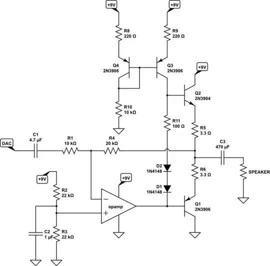
I'll try to include as much information as I can here to facilitate understanding what I can do and where the issue could be. Below is a schematic of the top level of my design. You can see many of the ports are assigned a fixed value so I don't have to worry about them inside the controller, such as the CKE and CS_N signals, as well as the input/output masks.
Below is a state diagram I've developed for my sdram controller. Two details I haven't included in it are the reset signal, which always resets the counter and puts the controller back to the POW state, and the fact that the counter is incremented when transitioning to the INIT3, WRIT2 or READ4 states, or at every cycle when at the POW state. Please note that the SDRAM chip used only samples inputs during positive clock edge.
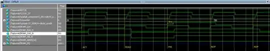
Below are a some of the simulations I've made. I've manually added some guides in the images to point out the moment the DRAM_CLK port receives a positive edge, and the command the controller must have sampled. KEY[3] controls the Reset_n signal. CLOCK_27 is the native board oscilator, and bellow it is the output of the PLL component that feeds the controller. The counter register and the signal that identifies the READ4 state (necessary for outputting the valid signal) are there as well. The data being fed into the controller is arbitrary, and the address pins are being fed the value 0010 0010 0000 during MRS (and at any other moment really, aside from the occasional change in A10)
Initializing - End of 200us wait:
 Initializing - 8th refresh done, issuing MRS:
 Reading:
 Writing:
 Refreshing:
I'm hoping the provided information can give a clue to what's going on, or to what I can do to debug this. I really just want to have this working, but am clueless as to what's going wrong.