0

At the beginning of the circuit, I designed a 20Hz to 20kHz second-order Butterworth bandpass filter circuit, and then I tried to pass the filtered signal through an AGC circuit to achieve a smooth output.

I tried frequency domain simulations with different amplitudes on CircuitLab, but I don't know why the output showed the same gain. In this AGC circuit I'm using a TL071 op-amp (was originally going to use a NE5534). R3 and J1 form an amplifying circuit. Through the envelope detection circuit formed by D5, R5 and C4, the output AC signal is converted into a DC signal and input into the gate of J1 to achieve the effect of controlling the gain with the change of the signal amplitude.

Is there any problem with the AGC circuit to give the output same gain instead of more gain for smaller input and less gain for larger input?
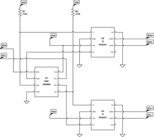
enter image description here

enter image description here

JRE
  • 67,678
  • 8
  • 104
  • 179

2 Answers2

1

Frequency domain analysis linearizes the circuit at the operating point. I'm afraid the program you used finds the operating point with DC analysis and by assuming the input amplitude is zero - no matter how many volts you have written for your signal source. The small signal frequency domain analysis is performed only in that operating point. It knows nothing of what happens with large input signals, the whole AGC attempt stays hidden.

Do the analysis in time domain to see what actually happens. Simulate like you had a built circuit, a signal generator and an oscilloscope. I guess you are also interested in or at least should be interested in how stable is your gain control feedback loop, how it responds to fast and slow signal amplitude variations and how much it distorts the signal vs. frequency. Time domain analysis can reveal them all if you use enough different test signals.

About the design: Qualitatively it can work. It makes the gain reducing feedback stronger for the rightmost opamp as the input signal amplitude grows. And the gain returns as the charge decays in the smoothing capacitor C4.

The rightmost stage cannot make its voltage gain lower than 1 which can be less than ideal.

The non-linearity of the ON-resistance of the JFET can be a real problem with stronger than millivolt-level signals. The distortion can be intolerable. To avoid it check, if a LED-LDR pair could do what you expect. LDR is much more linear. It can also be a good idea to search for off-the -shelf IC solutions for your AGC needs.

1

with the FET off, the output stage has unity gain. As you apply a larger signal, you apply negative volts to the gate, which (presumably, I didn't check if you are using the correct type of FET) starts to to turn it on. This will INCREASE the gain of the output stage. This is not an AGC (i.e. type of compressor) circuit, it is an expander. Once you start applying enough signal, the output gets larger until saturation.

Also, as others have pointed out, the frequency domain analysis of this circuit is not really connected to what you are trying to do with AGC. They are two separate problems (apart from making sure you have reasonable frequency response, and choosing the time constant of your detector (diode/R/C) stage.

I didn't check the values of R and C or that you are using an appropriate FET to give voltage controlled resistance. But your basic topology looks wrong. You need gain to reduce as signal gets hotter.

(Assuming that the FET is reducing in resistance as signal level rises, the easiest way to do this is to use it as the ground resistor in a potential divider, which attenuates the signal applied to the final stage, which can now just be a fixed gain buffer.)

danmcb
  • 6,009
  • 14
  • 29