3

I am trying to make a simple class A audio amplifier with one transistor (TIP41, NPN) in common emitter configuration as shown in the pictures.

circuit when idle/ no input signal

The problem I have is that when I add the input signal (more than 1 V), the transistor's base bias changes quickly from positive to negative in such a way that no usable amplification is possible. I can get 1 V/0.2 A output at best from the 10 V/0.57 A supply input. That's 3.5% efficiency.

circuit under 1V audio input signal

Should the input signal stay under 1 V, is that the cause of bias change? Is the signal too strong for this base bias current? If so, how are signals amplified further (in large amplifiers,) if the final stages can't take more than 1 V or close? It can't be right.

JRE
  • 67,678
  • 8
  • 104
  • 179
  • 4
    Well, larger amplifiers aren't typically single-transistor class-A designs, so the question "how are in large amplifiers signals amplified further" might be answered with "by using a different design that doesn't have as bad an efficiency". Also, this would seem to be like a mid-60s design: humongously strong base bias resistors, no feedback whatsoever, a transistor with a hFE < 100 … – Marcus Müller Feb 22 '23 at 17:55
  • 2
    [What is the purpose of the emitter resistor in a common emitter amplifier](https://electronics.stackexchange.com/questions/556899/what-is-the-purpose-of-the-emitter-resistor-in-a-common-emitter-amplifier/556905#556905). – Andy aka Feb 22 '23 at 18:27
  • You need an oscilloscope. When you drive the input with large signals, output is distorted, and transistor operation has exited "Class A" - it is no longer a linear amplifier. An oscilloscope will reveal that output wave shape is not an inverted version of input wave shape. – glen_geek Feb 22 '23 at 19:03
  • @Marcus Müller Yes, the design and approach matters, I meant something probably unfeasible (how large signals are made/ amplified - NOT by cramming them into base-emitter circuits, I understand now) My montage is the classic one, from the books (so it is old, indeed), I want to see it working. – Alin Paladin Feb 22 '23 at 19:02
  • @Andy aka As I already said to ErnestoG, I will try this approach, thank you for the link. – Alin Paladin Feb 22 '23 at 19:02
  • What load do you have? A resistor loaded class A amplifier is not expected to have an efficiency of better than 12.5% under ideal conditions. The maximum input would be about 50-100mV p-p before distortion sets in. – Kevin White Feb 22 '23 at 19:21
  • @glen_geek - I don't have an oscilloscope right now, although I can makeshift one via computer and soundboard. I will check this after I succeed to drive correctly the transistor. – Alin Paladin Feb 22 '23 at 19:36
  • @Kevin White The load is a banal speaker, at 4 ohms. I know about Class A inefficiency, yet it is too much in my case - 3.5%. I will redo the circuit correctly (with emitter resistor), and then we'll see if it improves a bit. – Alin Paladin Feb 22 '23 at 19:37
  • **My montage is the classic one, from the books (so it is old, indeed), I want to see it working.** Did those books tell you how big of a signal this circuit can amplify? If not, you should look for better books. There is a lot of books that present trivial circuits that either don't work or barely work, or use parts impossible to get. Better yet, simulate your circuit - the best you can do before getting an oscilloscope. CircuitLab is included in the EE StackExchange question and answer editor so you can use it for free. Do use it! *And don't burn your fingers on this circuit :)* – Kuba hasn't forgotten Monica Feb 23 '23 at 02:36
  • @Kuba hasn't forgotten Monica Well, they said the transistor can amplify up to x100, which sounded good enough for me. Yes, I will check the CircuitLab, thank you for that. I am already trying an old software - Electronics Workbench, which sheds a bit of light into the matter, but obviously the CircuitLab is the better choice. – Alin Paladin Feb 23 '23 at 03:02
  • At the suggestion of Kuba hasn't forgotten Monica, I am trying CircuitLab. I can already see there is there even the type of transistor I am working with. It will be a matter of time until I will figure out what I am doing wrong in the circuit, and thus, my post should be considered as "resolved". Thank you to everyone for the help. – Alin Paladin Feb 23 '23 at 03:54

5 Answers5

3

This is happening because you're not using negative feedback.

For a common-emitter amplifier like this you need series-series feedback (AKA emitter degeneration). This will desensitize your transfer from beta (current gain) variations.

If you really need the gain, then you can also include a parallel capacitor with such resistor so that the emitter is grounded at AC (you still get the negative feedback at DC, so your transistor will be biased properly). However, this will make your AC transfer more sensitive to beta variations, so you'll suffer from more distortion.

Whatever you choose, you need feedback for linear amplification, there no other way.

If you must use stages like these for amplification, you can ditch the divider and make an inverting amplifier; connect the output to the 1st stage base node, and place another resistor in series so that you can define your gain as the classical inverting amplifier. This way you make good use of the large open-loop gain these common-emitter stages provide.

EDIT:

Perhaps I read your question too quick. If you're trying to have a predictable voltage gain and able to feed 3A into a load, there is no way you can do this with a single stage, much less with a textbook common-emitter amplifier.

The fundamental problem with a common-emitter amplifier is that, it's basically a transconductance amplifier with a predictable load (the collector resistor), i.e. it needs a predictable load for a predictable linear gain (and the quiescent collector current is fixed by the emitter voltage divided by the emitter resistor you added). You say you want to feed to a 4 ohm load that will be, effectively, in parallel with your collector resistor. Your gain will vary, and the current you have fixed with the series-series feedback (the emitter resistor) will now have to be shared among your load and collector resistor.

The only decent use for a common-emitter is as a preamplifier (or if your load is >2 orders of magnitude higher than your collector resistance), while subsequent buffer can provide the current capability you use.

I see you have agreed that you should change your approach for this design. Good luck!

Designalog
  • 3,232
  • 1
  • 13
  • 23
  • I will try to add this feedback resistor to the circuit. I knew about it, but I thought it is for overheat protection mainly. Maybe if I make the base to be at some positive potential through emitter resistance, the the bias will not drop anymore? - I will check this out. For start, I want to have a working model of one single transistor - you can tell why. In the specifications, this transistor handles up to 100 V/ 6 A / 65 Watts total. I wish to see that with my eyes - an output even of 12 V/ 3 A would be huge for me. – Alin Paladin Feb 22 '23 at 19:02
  • @AlinPaladin are you saying that your load is 4 ohms? (12V/3A) – Designalog Feb 22 '23 at 19:41
  • @AlinPaladin The 65 W is an **absolute maximum**. Same with 6 A. Same with 100 V. Note also that the 65 W only works ***if and only if*** you can somehow guarantee that the case stays at 25 C and that the chip die itself doesn't experience anything anywhere on it that goes over 150 C. The safe operating area spec points out the obvious: if the VCE > 10 V then the max current goes *down* and at 100 V can only be 200 mA. Note also that while (150 C - 25 C)/65 W suggests junction to ambient of >1.9, it is really a little better at about 1.7. But they are being safe, just in case. – periblepsis Feb 22 '23 at 20:06
  • @AlinPaladin Using a heat sink [like this](https://www.mouser.com/datasheet/2/2/Board-Level-Cooling-Extruded-5810-1275100.pdf) doesn't even specify it's dissipation in still air. But with a little bit of flow they give about 10 C/W. Then there's the thermal compound -- maybe another 0.5 C/W at a guess with a thin layer using 'good stuff'? So this is perhaps 10+0.5+1.7 or about 12 C/W from the die to air using that heat sink and a small breeze. Using a risky 100 C rise, which I would not do, and a fancy heat sink you might get about 8 watts out of it. Being conservative, half that much. – periblepsis Feb 22 '23 at 20:36
  • @AlinPaladin And that assumes your ambient is 25 C. Since it might operate in 55 C environs, you can use a risky (125 C - 55 C)/12 = 5.8 W or a less risky (85 C - 55 C)/12 = 2.5 W. The point of all this is to disabuse you of the idea that 65 W is practical. It's what the device might do if you could find a way keep ambient at 25 C (55 C isn't possible) and could find a thermal solution that adds no more than 0.22 W/C to the thermal resistance. Good luck with that! – periblepsis Feb 22 '23 at 20:55
  • ErnestoG@ I have added a 1.5 ohm emitter resistor and reduced the collector resistor to 8.5 ohms (from 10). Later I have added an additional 2.2ohms resistor to the 1.5 ohm emitter resistor. In each case the base bias voltage raised indeed, but the problem remained the same - the input signal once too large makes the base voltage to drop under 0. The total power output was unchanged -  around 0.2 watts. The only thing it did was to shift a bit the point in which the voltage drops - it reduced the gain, so it needed a bit more volume input. – Alin Paladin Feb 22 '23 at 21:32
  • ErnestoG@ For testing purposes, I have ramped up gradually the voltage supplied, up to 30 volts, to test if maybe it is an undervolting situation. After a point the base voltage rised over 0, it was in the "range" (over 0.7 V, under 2 V for this transistor), yet the power output didn't change much - maye it became 1 watt. At 30 volts there were weird readings over the base voltage - around 7-8 volts, yet the transistor is fine. The power output did not go over 2 wats - this at 32 volts and 2.5 amps supplied. – Alin Paladin Feb 22 '23 at 21:33
  • ErnestoG@ The testing load is a speaker, yes, at 4 ohms. The audio source used for the input has an output of 2.5 watts (4 V, 0.4 A) I understand ratings, of course. I don't expect to have 6 A at 100 V or something similar. But I can't extract more than 2 watts at 75 watts power supplied + 2.4 watts on the input, I don't get it. How is it supposed to reach that wattage rating, or, at least one quarter of it? Are the ratings only for switching mode? (on/off). The transistor is not broken, since the audio works fine at small volume. – Alin Paladin Feb 22 '23 at 21:33
  • @periblepsis - The transistor doesn't heat too much. It is bolted to a piece of aluminium, without thermal paste yet. It gets slightly warm, most of the power goes through resistors - they get hot. If I am right in my estimations, the transistor handles at most 10 watts when I dump 75 watts in the circuit - I don't have the right circuit yet, still trying to figure out. Until now, the transistor does nothing, max output from it was 2 watts out of those 65 advertised. – Alin Paladin Feb 22 '23 at 21:42
  • @AlinPaladin That's because the BJT is saturated out, looking at the design. So VCE is very small. – periblepsis Feb 22 '23 at 22:46
  • @AlinPaladin Do you want to drive a 4 Ohm speaker from a standard commercial (not professional) line output from some device? And do all of that, without noticeable distortion, from the use of a single BJT, some resistors and capacitors, and a 10 V supply rail? – periblepsis Feb 22 '23 at 23:02
  • @periblepsis Yes, I want to drive a 4 ohm speaker through a single (power) transistor stage. The common emitter configuration is supposed to do high amplification for both voltage and current. That is what I try to get - I give 1 V, 0.2 A input signal, the transistor modulates 4 V, 0.8 A in an almost identical wave (for class A). This is what I have understood about what transistors do. Where I am wrong, or what I am missing? – Alin Paladin Feb 22 '23 at 23:49
  • @AlinPaladin Most audio line levels are designed to drive a high impedance input, for example. When you write that you "give" 1 V, 0.2 A input signal this means to me that it's not the usual kind of line output from some typical device like a cell phone headphone jack. So what exactly are you using to drive it? Or is this to be an entirely hypothetical exercise? – periblepsis Feb 23 '23 at 00:55
  • @periblepsis I generate 50 Hz using an app on my tablet, then I send the tone to the circuit of a small audio system. The output on a 4 ohms speaker is around 0.4 A , 4.5 V, as best as my cheap multimeter can measure. The sound on this power level is good - no distorsions. I try to amplify that signal using the transistor. When I will be able to get the expected amplification out of a single transistor stage, I will make more stages, to have some speakers with their own mini amplifiers - somewhere in the 5 - 10 W range. – Alin Paladin Feb 23 '23 at 01:23
  • @AlinPaladin Was taking me a while to figure out where you were headed and it looks like you have an answer, for now. I was struggling to imagine how to write to you -- bridging some gaps. But wasn't ready, yet. Best wishes! – periblepsis Feb 23 '23 at 17:55
3

Have a look at the behaviour of this transistor, as its base voltage is changed. Here's the circuit with just the transistor and a collector resistor:
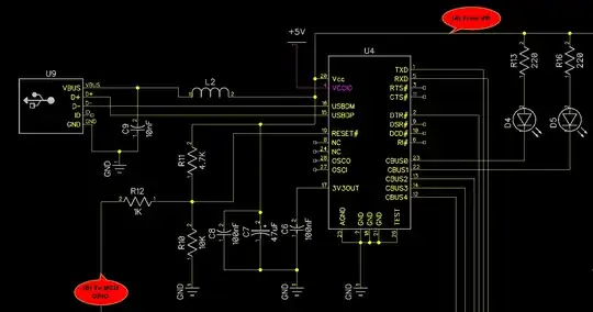
schematic

simulate this circuit – Schematic created using CircuitLab

This is what happens to the collector C potential, as the base B is swept from 0 to +1V (with respect to the emitter):
enter image description here

As you can see, the collector potential cannot ever rise above the positive supply of +10V, or below the emitter at 0V. This means that the only useful region of operation (from an audio perspective - digital is a different story) is in the part of this graph between the green markers.

Base potential must remain at all times between 0.67V and 0.75V, if you wish to avoid "clamping" the collector against either supply potential.

That's a range of less than 0.1V, so if you apply a signal with amplitude 1V, the base will spend most of its time well outside those limits, and the output will clamped to either +10V or 0V most of the time.

This common-emitter design is suitable only for very small amplitude inputs, significantly smaller than 0.1V.


Now let's address your biasing of the base, with resistors 690Ω and 620Ω. These form a potential divider, which will attempt to provide a potential about half way between the supplies, at the transistor's base. That's only an estimate, based on the similarity of their values, a simulation will show us the real value, on the left voltmeter:

schematic

simulate this circuit

That's already far above the 0.7V-ish point where you need the transistor's base to be "centered" around.

On the right is what happens to that potential with the transistor in place. The base and emitter of the transistor behave as if there was a diode between them (because, technically there is one), and this diode to "ground" prevents the base from rising much higher than 0.7V. Here the voltmeter shows 0.88V, which again is way outside the range of potentials you need to be providing at the base.

The transistor is clearly driven so hard into conduction, that its collector is super-glued to 0V. To get it out of this state would required a very strong input, able to pull very hard, downwards, the potential of the node at the resistors' junction and transistor base.

While what I am about to suggest is by no means a "good" solution, it might at least help you get somewhere with your experimentation. I suggest you change your resistances to try and achieve +0.7V at the base:

schematic

simulate this circuit

Have a play with the simulation, to see what voltages appear in various places as you change the resistances. Pay close attention to collector voltage too.


There are other issues, but these two must be fixed before I could begin to talk about the others. I hope you've got a better grasp why your circuit cannot hope to operate as an audio amplifier, in its current configuration.

Simon Fitch
  • 27,759
  • 2
  • 16
  • 87
  • 1
    Thank you very much for the efforts to explain to me the phenomenon - you gave me the best clarification posible. I am now able to fully understand the problems brought by voltage input. I will simulate on my own those three configurations possible for the transistors, to find what suits me best, and after that I will make probably a few complementary stages out of them. The topic can be closed I think, since the problem is solved for me. Thank you again to everyone. (edit: the other issues with the circuit will not be a problem anymore, now that I got the main mistake) – Alin Paladin Feb 23 '23 at 15:11
2

The problem I have is that when I add the input signal (more than 1 V), the transistor's base bias changes quickly from positive to negative in such a way that no usable amplification is possible.

This phenomenon is not so much related to transistor amplifier circuits but rather to diode rectifier circuits. There it has been known and used for a long time (especially in TV receivers) in the so-called "DC restoration circuits". Here is my explanation.

Equivalent circuit

With a large input signal, the base-emitter junction can be considered as a diode; so the input part of the circuit can be simplified to the following form.

schematic

simulate this circuit – Schematic created using CircuitLab

Simplified equivalent circuit

To see the basic idea clearly, we can simplify the circuit even more by removing the resistors and replacing the diode with an "ideal" one (VF = 0 V). Thus we obtain the following conceptual schematic.

schematic

simulate this circuit

During the positive half-wave, the diode is "on" and the capacitor quickly charges through it; during the negative half-wave, the diode is "off" and the capacitor has nowhere to discharge.

As a result, the capacitor remains permanently charged to a voltage equal to the peak of the input voltage. This DC voltage is subtracted from the input AC voltage and drops it below zero.

Graph_1 Extremely simplified equivalent circuit

In fact, the diode is permanently "off". So we can remove it from the circuit diagram and replace the charged capacitor with a constant voltage source with the same voltage Voff = Vc. Thus we get an extremely simple conceptual circuit diagram.

schematic

simulate this circuit

Graph_2

If we compare the two graphs, we see that they are the same except for the initial part where the capacitor must be charged.

Circuit fantasist
  • 13,593
  • 1
  • 17
  • 48
  • 1
    Thank you for your explanations. I have already got the reason why I can't go over some 0.1 V input, for the current common emitter configuration, from Simon Fitch, posted above. I know now where I was making mistakes - wrong transistor configuration for the input signal - that's why it didn't amplify a thing. I am pretty set now, with the explanations I got, and with the aid of the simulation software, I will search for the right transistor configurations for my particular requirements. The topic can be closed, and marked as solved. – Alin Paladin Feb 23 '23 at 15:25
  • Doesn't the first model place the output at the emitter, but it's really on the collector? – Scott Seidman Feb 23 '23 at 20:41
  • 1
    @Scott Seidman, I have considered the circuit of C, R1 and R2 as a *bias* (or *DC restoration*) circuit with its own input and output. I was hesitant to label it with BASE instead of OUT but I wanted it to be more symmetrical. Do you approve of my idea to present the input part of the circuit as a DC restoration circuit? It emerged in my mind from a very distant time (the 80s) when I was studying with interest the complex analog and pulse circuits of TV receivers. I think there were such detectors that used the base-emitter transition of the transistor as a diode... – Circuit fantasist Feb 23 '23 at 21:09
  • 1
    I missed the phrase "input side" in your post. With that, I think the post is OK, but would be clearer if you labeled the point V sub b, to match the original poster's notation. He uses "out" differently. – Scott Seidman Feb 24 '23 at 01:09
1

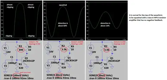
Your transistor has way too much base current causing its bottom of the output waveform to be clipping. Since it is class-A without any negative feedback then it is normal for the top of its output waveform to be squashed.

I do not has a model for a TIP41 so I used a similar transistor. There is a high range of the hFE of a transistor part number anyway that needs selection or DC negative feedback to be used.

The distortion sounds awful and the heating is absurd for the small amount of output power. It will have much more trouble trying to drive a speaker. class-A

Audioguru
  • 3,894
  • 5
  • 8
  • The circuit looks correct (it is like what I have), and I am sure the different model used doesn't change things that much, yet I say I had 1 V input without audible distorsions (before modifications). Now, with some resistances added to the emitter, audio works fine up to 3 V! input (but the power output is the same - 0.2-0.4 W). Signal used is 50 hz, multimeter shows 3 V at the input point. Unfortunately I don't have something better than a regular multimeter, that's why I do measurements at 50 Hz, it is it's expected working frequency. – Alin Paladin Feb 22 '23 at 22:04
  • A multimeter cannot measure distortion. Since the amplifier distortion is so high then the multimeter also cannot correctly read the output volts and amps. At 50Hz the output capacitor is 32 ohms. Most multimeters read volts RMS which is 0.707 times the peak voltages in my simulations that show about 60% distortion when the input is only 40mV peak which is 28.3mV RMS (0.0283V RMS). I forgot to say that the input resistance of your amplifier is VERY low, about 30 ohms. – Audioguru Feb 22 '23 at 22:59
  • My multimeter is a cheap one, which gives orientative readings. Of course I can't measure distortion with it, but what preoccupies me the most is the lack of power. Even with the approximate readings, for 15 watts in, I get 0.2 watts out, no distorsions. For 80 watts in, I get 1.5 watts out, no distorsions heard - sound is good. I say there's a problem either with the montage, either with my expectations about how much amplification a transistor can give. – Alin Paladin Feb 23 '23 at 00:13
  • Your problems are caused by using cheap and antique class-A. – Audioguru Feb 23 '23 at 01:18
  • @ Audioguru I agree that this kind of montage is obsolete, yet I wish to see it working, as it is depicted in the specifications. That is the main point - it is said that one transistor can handle a current up to 100 times the input, for example. I want to have a working model of that, with as few components as they are in the diagrams. The type I am using is said to modulate 6 A/ 65 W. Well .. I want to see those numbers, one way or another. I can't take "max 0.3 A, 2 W" as an answer. – Alin Paladin Feb 23 '23 at 01:41
  • @Audioguru Add a diode across that capacitor, it is polarized after all! – Kuba hasn't forgotten Monica Feb 23 '23 at 02:40
  • The datasheet for the TIP41 transistor says that with Vce at or more than 4V and a collector current of 3A then the minimum hFE is 15 and the maximum is 75, NOT 100 times. You do not know the gain of your transistor unless you test it. A good reason to use DC negative feedback. For a peak of 6A into your 4 ohms speaker then it needs to be fed a peak of 6A x 4 ohms= 24V but the 10 ohms resistor is in series needing an additional 6A x 10 ohms= 60V. So the power supply must be 24V + 60V= 84V which is crazy. – Audioguru Feb 23 '23 at 23:44
  • The TIP41 must feed an additional current of 24V/10 ohms= 2.4A into the 10 ohms resistor for a total current of 8.4A peak which will destroy the little TIP41. A class-AB amplifier replaces your class-A power wasting 10 ohms resistor with a PNP transistor that can apply +24V to the speaker without adding more current when the tIP41 pushes down the speaker to a peak of -24V. Then the output power into the 4 ohms speaker can be 72W when the power supply produces about 54V. – Audioguru Feb 23 '23 at 23:49
1

The input \$1000\mu F\$ capacitor (I suspect is polarized) is correctly biased when the input is 1V. When 0V is applied the capacitor is essentially a short.

The input voltage must be less than 500 mV.

Edit: This also explains why an emitter resistor allows a higher input voltage.

RussellH
  • 12,496
  • 2
  • 9
  • 34
  • Capacitor is there only to stop DC going from one circuit to another. I have tried to reduce the input voltage (by using resistors), but this doesn't make the transistor operate any better - from the output of 0.2 watts at 10 V, it drops to insignificant amounts. The transistor is rated to 65 watts, I expect more than what currently does - I gave it 30 V, 2.5 A ,it has outputted 2 watts clean sound - obviously something is wrong, that's not amplification by any means. Even the input source does more than that, with way less power. – Alin Paladin Feb 23 '23 at 00:24
  • Your problems are caused by using cheap and antique class-A. – Audioguru Feb 23 '23 at 01:17
  • 1
    Electrolytic capacitors block dc in one direction only @AlinPaladin – RussellH Feb 23 '23 at 01:58
  • @RussellH What is that direction please? I was expecting to have it blocked in any direction? The collector bias gets blocked like this - until I have added the decoupling on the output, the current bias flowed into the speaker, now it doesn't. Also, speaking about, I have tried an old software (Electronics Workbench) and it seems that there are indeed some problems with both capacitor value and input signal value (no more than a few hundred mV), I will work more on that. In practice it didn't appear so, I have to check it more thoroughly now. – Alin Paladin Feb 23 '23 at 02:26
  • Do you understand the difference between polarized anf non-polarized capacitors @AlinPaladin? – RussellH Feb 23 '23 at 02:34
  • 1
    @AlinPaladin You really should draw the "+" symbol on the schematic, in agreement with the polarization of the capacitor in your circuit! The capacitor behaves like a capacitor when the "+" terminal is higher than the "-" terminal. When the voltage across the polarized electrolytic capacitor is reversed, it will act as something else, but definitely not a capacitor anymore. – Kuba hasn't forgotten Monica Feb 23 '23 at 02:38
  • @RussellH Non polarized capacitors work both in AC and DC, polarized ones get shorted in AC, and they also get damaged in DC if they are connected backwards. For me, they seem to behave like a battery/ acumulator in this matter. I am using electrolytics for decoupling because it appeared that they may be used like this (in series), at least temporarily, without being damaged. In parallel they would have been blown in seconds. – Alin Paladin Feb 23 '23 at 02:45
  • @Alin Paladin Polarized capacitors work only when properly biased. You should mark their polarity as suggested by Kubahasn'tforgottenMonica – RussellH Feb 23 '23 at 02:49
  • @Kuba hasn't forgotten Monica I forgot to mark the capacitors when I made the drawing, and later when I realised that, I thought it was not that important anyway, since they worked without noticeable effect in both ways. I have asked myself what would be the right way to place them, but since I can't get the "amplifier" to work at all, I have put this in second place. People say it's best to use two, in series, if they are meant for a long term, but I didn't get there yet. I will revise everything now, since it appears that they have an influence on the transistor's wave output. – Alin Paladin Feb 23 '23 at 02:56