• Is this a practical way to work around the low current ratings of multiplexers?
• Is this a proper application of a PNP transistor?
It's a decent solution. You've created a PNP "emitter follower" (also called common collector) amplifier circuit to buffer your multiplexer output. This is also known as a "Class A Amplifier" and one of the first things you notice when you start reading up on this type of amplifier is that they are power inefficient. It's especially true in this case since your load is DC coupled, when most Class A amps have AC coupled loads. Basically, this means your PNP transistor is going to burn up extra heat in proportion to how much current needs to flow through your LED.
• The values of the resistors are pretty low, but the circuit seemed to
function as I intended with almost no change for extremely high
values, how would I know what a proper value for the resistors could
be?
I'm not sure which resistors you're referring to. R1 is mostly going to set your LED brightness, so that one might have to be done experimentally. It's going to be highly dependent on the rest of your circuit, so maybe that one is best doing last. Make sure you pay attention to how much power that resistor is dissipating so you can select the correct wattage. The base resistors for the NPN transistors are going to depend on how hard you want to drive the transistors. You didn't make it clear if R2 and R3 are embedded into the controllers, so I'll ignore those assuming they are. R4 and R5 are going to effect how well your Q3 NOT gate is going to work in terms of switching speed and how much current to want use up from your GPIO pin when it's on. You can probably get away with 1K on the collector and 10K on the base. You should experiment yourself and see what works best for you. The collector resistor will also determine how much power you'll draw from the 12V rail when the transistor is on.
• I tried to find a more accurate LED model but I'm a little lost. The
LEDs I'm controlling are embedded in a larger component and I'm having
a hard time finding how to determine the necessary values for
simulation. I'm willing to pretend it's a 12V strip with 5050 RGB LEDS
that is 3 LEDS in length. Note LEDS would be 4-pin RGB with common
anode, not 3-pin ARGB
Creating your own SPICE model is not going to be that easy. I don't know anything about RGB LEDs. If you think they are effectively 3 LEDs in series, then I would pick 3 LEDs from the built-in LTspice model library and connect them in series. You can try to do more bench experiments to gather more info or try to find a datasheet for your LEDs.
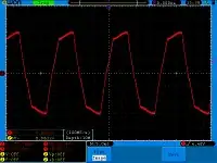
• When the multiplexer source is changed from the GPIO the spice sim
showed a nasty current spike (pictured in second image), how can I
prevent this spike?
You didn't explain through what component the spike is occurring through. It's likely due to the rapid switching between the two sides of the MUX. Slowing down the switching can reduce or eliminate this.
• The Input control of the multiplexer is controlled by a not gate, is
this a proper implementation? Is it necessary for a chip like the
TMUX4053 that offers 1.8V logic compatible thresholds?
It's unnecessary for either the ADG1236 or TMUX4053. You need to look at the \$V_{IH}\$ and \$V_{IL}\$ parameters in their datasheets and see if you meet the requirements. From what I can tell, a 3.3V GPIO from a CMOS microcontroller should be able to satisfy both requirements for either part.
• Is there a better way to switch between 2 low side switches?
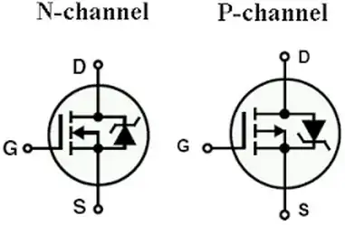
Yes...two more low side switches in series with the existing ones. I think you're wasting effort with the analog switch (multiplexer). Analog CMOS switches are meant for switching voltages throughout the entire power rail swing (in this case: 0V through 12V). Since you're switching point is the collector of a emitter-grounded NPN transistor you only need to switch a few millivolts (due to \$V_{CE(sat)}\$) above ground. An analog CMOS switch is constructed with an N-channel MOSFET and P-channel MOSFET in parallel. The idea is that the N-channel is used for the low-side voltages and the P-channel for the high-side voltages and they work together in varying degrees for the values in the middle. Since you only need the low-side switching, you only need the N-channel half of it...so just use that half. Put another way, you can replace your SPDT switch (multiplexer) with two SPST switches (two discrete transistors).
In the comments you mentioned you are uncomfortable using MOSFETs, so we'll use NPN BJTs as the low-side switches. You also said you can use an additional GPIO pin from your microcontroller which will make the control easier and more customizable. This way you can turn one switch off in software, and then delay for a few clock cycles before you turn the next one on...and so forth. Below is an example using 2N3904 BJTs (image and also the LTspice .ASC file pasted as text):
Version 4
SHEET 1 1204 680
WIRE -64 -512 -128 -512
WIRE 96 -512 16 -512
WIRE 240 -512 160 -512
WIRE 384 -512 304 -512
WIRE 560 -512 448 -512
WIRE -128 -480 -128 -512
WIRE -128 -368 -128 -400
WIRE 560 -352 560 -512
WIRE 560 -352 64 -352
WIRE 1104 -352 560 -352
WIRE 64 -256 64 -352
WIRE 1104 -256 1104 -352
WIRE -112 -208 -176 -208
WIRE 0 -208 -32 -208
WIRE 928 -208 864 -208
WIRE 1040 -208 1008 -208
WIRE -176 -176 -176 -208
WIRE 864 -176 864 -208
WIRE -176 -64 -176 -96
WIRE 864 -64 864 -96
WIRE 64 32 64 -160
WIRE 1104 32 1104 -160
WIRE -160 80 -304 80
WIRE -112 80 -160 80
WIRE 0 80 -32 80
WIRE 880 80 736 80
WIRE 928 80 880 80
WIRE 1040 80 1008 80
WIRE -304 128 -304 80
WIRE -160 128 -160 80
WIRE 736 128 736 80
WIRE 880 128 880 80
WIRE 64 176 64 128
WIRE 1104 176 1104 128
WIRE -304 256 -304 208
WIRE -160 256 -160 208
WIRE 736 256 736 208
WIRE 880 256 880 208
FLAG -304 256 0
FLAG -160 256 0
FLAG 64 176 0
FLAG 736 256 0
FLAG 880 256 0
FLAG 1104 176 0
FLAG -176 -64 0
FLAG 864 -64 0
FLAG -128 -368 0
FLAG -176 -208 GPIO1
FLAG 864 -208 GPIO2
SYMBOL voltage -304 112 M0
WINDOW 123 0 0 Left 0
WINDOW 39 0 0 Left 0
SYMATTR InstName V1
SYMATTR Value 3.3
SYMBOL res -176 112 R0
SYMATTR InstName R1
SYMATTR Value 10k
SYMBOL res -16 64 R90
WINDOW 0 0 56 VBottom 2
WINDOW 3 32 56 VTop 2
SYMATTR InstName R2
SYMATTR Value 220
SYMBOL npn 0 32 R0
SYMATTR InstName Q1
SYMATTR Value 2N2222
SYMBOL voltage 736 112 M0
WINDOW 123 0 0 Left 0
WINDOW 39 0 0 Left 0
SYMATTR InstName V2
SYMATTR Value PULSE(3.3 0 12.5m 10u 10u 12.5m 25m)
SYMBOL res 864 112 R0
SYMATTR InstName R3
SYMATTR Value 10k
SYMBOL res 1024 64 R90
WINDOW 0 0 56 VBottom 2
WINDOW 3 32 56 VTop 2
SYMATTR InstName R4
SYMATTR Value 220
SYMBOL npn 1040 32 R0
SYMATTR InstName Q2
SYMATTR Value 2N2222
SYMBOL voltage -176 -192 M0
WINDOW 123 0 0 Left 0
WINDOW 39 0 0 Left 0
SYMATTR InstName V3
SYMATTR Value PULSE(3.3 0 70m 10u 10u 70m 140m)
SYMBOL npn 0 -256 R0
SYMATTR InstName Q3
SYMATTR Value 2N3904
SYMBOL res -16 -224 R90
WINDOW 0 0 56 VBottom 2
WINDOW 3 32 56 VTop 2
SYMATTR InstName R5
SYMATTR Value 1k
SYMBOL voltage 864 -192 M0
WINDOW 123 0 0 Left 0
WINDOW 39 0 0 Left 0
SYMATTR InstName V4
SYMATTR Value PULSE(0 3.3 71m 10u 10u 68m 140m)
SYMBOL npn 1040 -256 R0
SYMATTR InstName Q4
SYMATTR Value 2N3904
SYMBOL res 1024 -224 R90
WINDOW 0 0 56 VBottom 2
WINDOW 3 32 56 VTop 2
SYMATTR InstName R6
SYMATTR Value 1k
SYMBOL voltage -128 -496 R0
SYMATTR InstName V5
SYMATTR Value 12
SYMBOL res 32 -528 R90
WINDOW 0 0 56 VBottom 2
WINDOW 3 32 56 VTop 2
SYMATTR InstName R7
SYMATTR Value 82
SYMBOL LED 96 -496 R270
WINDOW 0 32 32 VTop 2
WINDOW 3 0 32 VBottom 2
SYMATTR InstName D1
SYMATTR Value QTLP690C
SYMATTR Description Diode
SYMATTR Type diode
SYMBOL LED 240 -496 R270
WINDOW 0 32 32 VTop 2
WINDOW 3 0 32 VBottom 2
SYMATTR InstName D2
SYMATTR Value QTLP690C
SYMATTR Description Diode
SYMATTR Type diode
SYMBOL LED 384 -496 R270
WINDOW 0 32 32 VTop 2
WINDOW 3 0 32 VBottom 2
SYMATTR InstName D3
SYMATTR Value QTLP690C
SYMATTR Description Diode
SYMATTR Type diode
TEXT -280 40 Left 2 ;Controller0
TEXT 760 48 Left 2 ;Controller1
TEXT 304 360 Left 2 !.tran 1
RECTANGLE Normal 160 0 -400 304 2
RECTANGLE Normal 1200 0 208 304 2
One other option is to use the single GPIO and invert it using an NPN inverter. The NPN inverter is so slow that the inherent delay will cause the first one to turn off before the 2nd turns on. The delay is a function of the resistors though, so you have to play around with those to get what you want. The 2 GPIO pins with software control option is easier in that respect.
Version 4
SHEET 1 1204 680
WIRE -64 -512 -128 -512
WIRE 96 -512 16 -512
WIRE 240 -512 160 -512
WIRE 384 -512 304 -512
WIRE 560 -512 448 -512
WIRE -128 -480 -128 -512
WIRE 560 -384 560 -512
WIRE 560 -384 64 -384
WIRE 1104 -384 560 -384
WIRE -128 -368 -128 -400
WIRE 784 -336 560 -336
WIRE 560 -304 560 -336
WIRE 784 -304 784 -336
WIRE 64 -256 64 -384
WIRE 1104 -256 1104 -384
WIRE -128 -208 -176 -208
WIRE -112 -208 -128 -208
WIRE 0 -208 -32 -208
WIRE 784 -208 784 -224
WIRE 1040 -208 784 -208
WIRE 560 -192 560 -224
WIRE 784 -192 784 -208
WIRE -176 -176 -176 -208
WIRE -128 -144 -128 -208
WIRE 608 -144 -128 -144
WIRE 720 -144 688 -144
WIRE -176 -64 -176 -96
WIRE 784 -64 784 -96
WIRE 64 32 64 -160
WIRE 1104 32 1104 -160
WIRE -160 80 -304 80
WIRE -112 80 -160 80
WIRE 0 80 -32 80
WIRE 880 80 736 80
WIRE 928 80 880 80
WIRE 1040 80 1008 80
WIRE -304 128 -304 80
WIRE -160 128 -160 80
WIRE 736 128 736 80
WIRE 880 128 880 80
WIRE 64 176 64 128
WIRE 1104 176 1104 128
WIRE -304 256 -304 208
WIRE -160 256 -160 208
WIRE 736 256 736 208
WIRE 880 256 880 208
FLAG -304 256 0
FLAG -160 256 0
FLAG 64 176 0
FLAG 736 256 0
FLAG 880 256 0
FLAG 1104 176 0
FLAG -176 -64 0
FLAG -128 -368 0
FLAG 560 -192 0
FLAG 784 -64 0
FLAG -176 -208 GPIO
SYMBOL voltage -304 112 M0
WINDOW 123 0 0 Left 0
WINDOW 39 0 0 Left 0
SYMATTR InstName V1
SYMATTR Value 3.3
SYMBOL res -176 112 R0
SYMATTR InstName R1
SYMATTR Value 10k
SYMBOL res -16 64 R90
WINDOW 0 0 56 VBottom 2
WINDOW 3 32 56 VTop 2
SYMATTR InstName R2
SYMATTR Value 220
SYMBOL npn 0 32 R0
SYMATTR InstName Q1
SYMATTR Value 2N2222
SYMBOL voltage 736 112 M0
WINDOW 123 0 0 Left 0
WINDOW 39 0 0 Left 0
SYMATTR InstName V2
SYMATTR Value PULSE(3.3 0 12.5m 10u 10u 12.5m 25m)
SYMBOL res 864 112 R0
SYMATTR InstName R3
SYMATTR Value 10k
SYMBOL res 1024 64 R90
WINDOW 0 0 56 VBottom 2
WINDOW 3 32 56 VTop 2
SYMATTR InstName R4
SYMATTR Value 220
SYMBOL npn 1040 32 R0
SYMATTR InstName Q2
SYMATTR Value 2N2222
SYMBOL voltage -176 -192 M0
WINDOW 123 0 0 Left 0
WINDOW 39 0 0 Left 0
SYMATTR InstName V3
SYMATTR Value PULSE(3.3 0 70m 10u 10u 70m 140m)
SYMBOL npn 0 -256 R0
SYMATTR InstName Q3
SYMATTR Value 2N3904
SYMBOL res -16 -224 R90
WINDOW 0 0 56 VBottom 2
WINDOW 3 32 56 VTop 2
SYMATTR InstName R5
SYMATTR Value 1k
SYMBOL npn 1040 -256 R0
SYMATTR InstName Q4
SYMATTR Value 2N3904
SYMBOL voltage -128 -496 R0
SYMATTR InstName V5
SYMATTR Value 12
SYMBOL res 32 -528 R90
WINDOW 0 0 56 VBottom 2
WINDOW 3 32 56 VTop 2
SYMATTR InstName R7
SYMATTR Value 82
SYMBOL LED 96 -496 R270
WINDOW 0 32 32 VTop 2
WINDOW 3 0 32 VBottom 2
SYMATTR InstName D1
SYMATTR Value QTLP690C
SYMATTR Description Diode
SYMATTR Type diode
SYMBOL LED 240 -496 R270
WINDOW 0 32 32 VTop 2
WINDOW 3 0 32 VBottom 2
SYMATTR InstName D2
SYMATTR Value QTLP690C
SYMATTR Description Diode
SYMATTR Type diode
SYMBOL LED 384 -496 R270
WINDOW 0 32 32 VTop 2
WINDOW 3 0 32 VBottom 2
SYMATTR InstName D3
SYMATTR Value QTLP690C
SYMATTR Description Diode
SYMATTR Type diode
SYMBOL npn 720 -192 R0
SYMATTR InstName Q5
SYMATTR Value 2N3904
SYMBOL res 704 -160 R90
WINDOW 0 0 56 VBottom 2
WINDOW 3 32 56 VTop 2
SYMATTR InstName R8
SYMATTR Value 10k
SYMBOL voltage 560 -320 R0
SYMATTR InstName V4
SYMATTR Value 3.3
SYMBOL res 768 -320 R0
SYMATTR InstName R9
SYMATTR Value 1k
TEXT -280 40 Left 2 ;Controller0
TEXT 760 48 Left 2 ;Controller1
TEXT 304 360 Left 2 !.tran 1
RECTANGLE Normal 160 0 -400 304 2
RECTANGLE Normal 1200 0 208 304 2
I won't get too much further into it, but you can use N-channel MOSFETs for either option. The main benefits for using MOSFETs are: (1) that you don't waste any current driving the gate since it is voltage controlled instead of current controlled, and (2) you can acheive much lower voltage drop across the transistor (low Rds(on) versus Vce(sat)) resulting in less power dissipation in the transistor. Your currents are quite low and you don't seem concerned about battery life, so it looks to me these won't effect you much. Sounds like if you reduced power/voltage-drop in your transistors, you would have to just increase your LEDs' series resistor to keep the 60mA you want...effectively just moving where the power will be dissipated.


