3

enter image description here

I'm reverse engineering a MPPT charge controller. I looked at its PCB and I drew the schematic from it and I've been as thorough as I can (checking and cross-checking many times). I know the "Intermediate circuit" schematic is jumbled up, and this is because I don't understand this section of this circuit. I'm trying to understand this circuit and planning on redrawing the this section so the relative spatial positioning of the components makes sense.

I'm especially having trouble understanding how the transistors are supposed to perform any function if their bases are tied together in that manner. It makes no sense to me. Can anyone tell me what could be the possible function of such a transistor configuration?

Here is the rest of the schematic: enter image description here enter image description here

xrosaber
  • 125
  • 1
  • 6
  • 2
    You schematic is somewhat jumbled. Could you spend some time to pretty it up and arrange the component so that building blocks are obvious. Frequently I’ll sketch out a diagram then redraw it so it reads easily. In doing this can help in picking up translation errors. As drawn I think you’ve translated the transistor pinout incorrectly. They do not make sense. – Kartman Feb 18 '23 at 06:25
  • You really need to redraw this and separate wires and use net names. – Shredder Feb 18 '23 at 06:39
  • @Kartman I've checked the circuit again and the transistor pinouts are correct. I understand that the schematic is jumbled up but this is because I'm still in the process of understanding the circuit, and without that understanding I can't arrange the components so that the building blocks are clear. – xrosaber Feb 18 '23 at 12:35
  • It would probably help in the interpretation of the circuit if you used zener symbols for those many zener diodes you have. Similarly with "J10_GND" - surely your schematic capture app has zener & GND symbols! – brhans Feb 18 '23 at 13:48
  • And I think the best explanation for those transistors with their bases connected comes from Occam's Razor - you've either made a mistake, or you've left something out. – brhans Feb 18 '23 at 13:55
  • @brhans I've checked the circuit and there is no doubt that the bases of the transistors are connected to each other unless, for some unlikely reason, the actual pinout and the datasheet pinout do not match. I've realized that there is more I can do to make the schematic readable with what I do understand about it. I won't delete the question in the meantime in hopes of someone answering it. – xrosaber Feb 18 '23 at 15:27
  • 3
    Different manufacturers sometimes make different versions of "the same" transistor with alternative pinouts. In the past I've had the common "jellybean" 2N2222 and 2N2907 with some of them EBC and others BCE (not all from the same batch obviously). – brhans Feb 18 '23 at 18:56
  • 4
    @xrosaber The process I'd use in fixing the schematic is to start by ***removing*** the bused power and just annotating, instead. You have a wire that goes from the +PV and +BAT and the cathode ends of six diodes that is NOT NEEDED!! It's just a +V rail. But the wire is running all over the place making the rest of the schematic hard to read. Start by labeling and getting rid of non-signal wiring. – periblepsis Feb 18 '23 at 20:50
  • 1
    @xrosaber Also, ***do the obvious***! You have an AMS1117 IC with its input tied to R11 and B_C2. It's input is also apparently protected by a pair of zeners. But you could reasonably leave those off or else re-arrange your schematic so that this looks more normal to read. I'm sure you could figure out that part because this is pretty easy. As you tease apart the Gordian Knot this way, stuff almost starts to align itself more automatically and you begin to ***see***. But get started with the obvious stuff. – periblepsis Feb 18 '23 at 20:54
  • 1
    @xrosaber Also, can you see on your schematic that NV_C1 is parallel to B_C2? Not easily. That's a problem. One thing you started doing right was to use J10_GND. But then you just wire it all over the place rather than getting rid of those wires and just using J10_GND label where needed. A LOT of wire clutter would be removed just doing that much. The point here is that these are things you can do. I know you can. But you are leaving all this to the rest of us. That's not fair of you. Put in more effort. It doesn't have to be perfect. But it can be better than what we see now. – periblepsis Feb 18 '23 at 22:16
  • @xrosaber I've not carefully looked over your update. But just a glance at it means +1 to me. So there's that, anyway. Thanks for the effort. You are still asking about the bases being tied together, I gather. Just those on the top schematic? – periblepsis Feb 20 '23 at 20:43
  • @periblepsis Yep, I'm still hoping to get an answer as to why the in the top schematic (labeled as "intermediate circuit") the bases are being tied together. – xrosaber Feb 21 '23 at 03:31

1 Answers1

4

In a quick scan of your schematic, I worry when I see things like this:

enter image description here

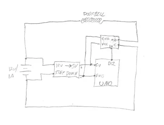
Should that be dotted? If not, is there really a \$500\:\Omega\$ resistor in series with a \$10\:\text{nF}\$ cap? Regardless of the answer, this particular area should be cleaned up so that it is clear to anyone reading it. It's not, as shown.

Don't bus around power -- within limits. Since this is a schematic about power, the rule is a little more nuanced because it may be important to highlight certain aspects of wires carrying power. But in general, to clean up the schematic you do need to do something to help.

Here's an example, below. I'm not offering it as the ultimate answer, but only as a starting approach. You've already provided a new label, J10_GND, that could be used for the negative PV rail. Why not use it to remove some of the rest of your wiring, instead of busing around all that wire?

schematic

simulate this circuit – Schematic created using CircuitLab

One thing that's made clear is that the (+) rails are tied together but that the (-) power rails aren't.

Note also that I've provided a couple of examples from the schematic that you could isolate for clarity. They tie directly to some interesting rails and are suggestive, already.

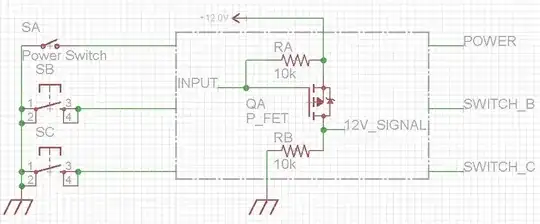
An oddball is your \$15\:\text{V}\$ zener, \$D_8\$, and the \$R_{25}=680\:\Omega\$ resistor. Certainly, the resistor value is consistent with the kind of current limiter one would expect for the zener. But look at what you have the other end of \$R_{25}\$ hooked up to! The base of a transistor, \$Q_{19}\$, and \$R_5=10\:\text{k}\Omega\$! How is that going to work, exactly? How will \$R_{25}\$ be fed the current we might expect if the only possible sources are either a BJT base or a \$10\:\text{k}\Omega\$ resistor??

As you pull things apart, piece by piece, you increase readability and understanding.

I believe that this will also begin to highlight better the sections you wonder about. It may be the case that when neatly separated out you'll realize that you may have the pins incorrectly identified. Whether or not, and where, will become clearer as you pull things out into nice sections that you do understand because those parts that now make better sense will help inform those remain bits that seem odd or less clear.

It's a process. Follow it through.

periblepsis
  • 3,766
  • 1
  • 1
  • 10