7

I am working on a project for LED control with MCU and LED drivers. I have an input voltage of 24 V and a DCDC converter to 3.3 V for the MCU. Each LED controller will have an output current of 1 A.

I searched all over the Internet and could not find a definite answer to the clearances rules, or the width of the trace, etc.

What are good rules to start with and so I can learn how to find specific values for these rules?

Null
  • 7,448
  • 17
  • 36
  • 48
Urban
  • 153
  • 4
  • 1
    this is far too broad; you'll want to read a book, not hope that someone copies a book on circuit design and board layout into the answers to a comment here. – Marcus Müller Feb 16 '23 at 10:14
  • Can you suggest a book that could help? I do understand electronics, I studied it, and worked as a schematic designer, but just started doing PCB layouts myself. – Urban Feb 16 '23 at 10:17
  • 3
    Awesome! So you're far more ahead of the curve than I thought! If you've designed circuits, that means you understand *why* you do things like place capacitors close to devices, and where what current flows. Now, you know *why* you want traces to have a some clearance – isolation. There's a buttload of calculators out there for clearance needs to be safe against creepage. In short, at 24V and below, you won't have a problem. Same for trace widths: you know *why* you need wide traces, resistance/voltage drop; there's a buttload of calculators for that out there, too. Generally, a trace that's – Marcus Müller Feb 16 '23 at 10:20
  • 3
    too wide doesn't hurt much (aside from making layout more complicated, potentially, if things start to get crammed). You design your traces to be wide enough so that the voltage drop doesn't matter to your use case. As the circuit designer, you're the only one who knows what that means – a 0.2Ω trace in series with a 10 kΩ resistor doesn't matter much, but in series with a 0.1Ω current sensing shunt, it does. That's basically all there is to it (at least for non-RF circuits). – Marcus Müller Feb 16 '23 at 10:20
  • 4
    IPC-2221 is a standard for all things PCB. You can d/l the "a" version I believe. Tables of creepage and clearance are contained. – Andy aka Feb 16 '23 at 10:24
  • 6
    It's possible that your PCB manufacturer will have a set of suggested design rules. – pjc50 Feb 16 '23 at 10:25
  • Thank you. Yes, I understand the reason why. But I just don't know the specific values I should put in as a design rule in Altium. So from what I was able to find the 0.15mm clearance is enough for up to 24V? I now used 0.5mm for 1A trace and 0.254mm for signals without much current. Great, thank you for your answer. – Urban Feb 16 '23 at 10:49
  • As well as the excellent comments above, look around at various PCB fabrication houses and their published technical specifications so that you're not designing right up to their limit for no reason. Some I've used are at [this manufacturer](https://www.pcbtrain.co.uk/pcb-design-rules) and [this one](https://eu.beta-layout.com/pcb/technology/presettings/) and made sure I was nowhere near their limits. – jonathanjo Feb 16 '23 at 13:29
  • Be sure to consider the voltage drop. Also, be conservative if you can. The tables will assume 10 degC temperature rise (or more). Do you really want your traces to be warm? Go 4X wider and you will have a few degrees temp rise. – Mattman944 Feb 16 '23 at 13:57
  • @Urban - Hi, You posted an answer saying thank you. The sentiment is appreciated, but that isn't an *answer* on Stack Exchange so it has been deleted, sorry. Please see [this page](/help/someone-answers) from the [help] (which is linked from the [tour]) explaining what to do when someone answers your question. If you don't need further help, please consider "[áccepting](https://meta.stackexchange.com/q/5234)" your choice of the best answer (i.e. click the "check mark" next to that answer, to turn it green) to indicate that your question has been solved. Thanks. – SamGibson Feb 16 '23 at 14:55
  • Your fabricator's recommendations are a good starting point for minimum distances and widths. Anything they can't fabricate you shouldn't make. I like to avoid getting too close to the minimum as well if you can avoid it it. – user1850479 Feb 16 '23 at 15:55

3 Answers3

7

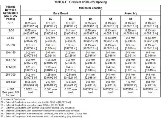
The below image is table 6-1 from the IPC-2221 standards. These are the minimum conductor spacings as a function of the voltage between two conductors, for various scenarios:

IPC-221 table 6-1

In my experience, these values work fine for "device in typical environment." Due consideration is still required for ESD-prone, isolated (high-voltage, low-nose, RF), and dynamic sections of the circuitry, as well as the environmental range expected (i.e. if there is a chance the circuit could ever exceed an altitude of 3000m, then design for it.)

rdtsc
  • 15,913
  • 4
  • 30
  • 67
  • I'm a bit confused about 'uncoated' vs 'polymer coating'. Does soldermask qualify as coating (it's a polymer after all) or do they mean conformal coating? I would expect three different values for bare copper vs soldermask vs soldermask+conformal coating – Gnarflord Feb 16 '23 at 18:52
  • 1
    I am curious about your "altitude of 3000m" exemple : what happens then? – Olivier Dulac Feb 16 '23 at 19:44
  • Gnarflord, I take "permanent polymer coating" to be akin to total encapsulation as the specs are nearly as good as "internal conductors." Olivier, at high altitudes there is less air to prevent arcing. Imagine a 275V trace with a clearance of 1.25mm for an LCD CCFL backlight. This is fine for sea level (B2.) But have a mountain climber take that device with them (B3) and this is not enough clearance distance.; the trace will likely fail. – rdtsc Feb 16 '23 at 21:39
  • 1
    Above 3000 m the air pressure is less and Paschen's law applies https://en.m.wikipedia.org/wiki/Paschen%27s_law – D Duck Feb 16 '23 at 23:22
  • @rdtsc I've studied the standards in depth, and I'm 100% confident that soldermask definitely qualifies as "polymer coating" under IPC. But IPC is NOT a safety standard, only a PCB quality control standard. If there's a shock hazard, it needs to be certified according to IEC standards, more rigorous electrical spacing is required. For more information, see my answer [Does recommended creepage distance apply to copper planes under soldermasks?](https://electronics.stackexchange.com/questions/583224/does-recommended-creepage-distance-apply-to-copper-planes-under-soldermasks/638830#638830). – 比尔盖子 Feb 17 '23 at 06:54
  • Right, I wasn't talking about shock hazards, but physical design limits. Often manufacturers will coat such traces in silicone to mitigate both. – rdtsc Feb 17 '23 at 13:12
  • What I wanted to say is that, because IPC is not a safety but a quality standard, this allows them to assign some pretty optimistic electrical spacing requirements. Such as classifying "normal" solder mask as a type of "permanent polymer coating", and giving design limits that are nearly as good as "internal conductors." A more conservative standard would refuse to consider solder mask and would only accept "proper" conformal coating - but IPC apparently has confidence in plain solder mask. As a result, depending on applications, it may or may not be good enough, even without consider safety. – 比尔盖子 Feb 21 '23 at 10:26
4

The IPC (formally the Institute for Interconnecting and Packaging Electronic Circuits) standards discuss minimum trace spacing and trace widths for circuit boards. They contain a lot of great information, but the standards are not free.

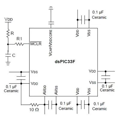
The Saturn PCB toolkit distills many of the IPC standards into what you need, and it is available for free:

https://saturnpcb.com/saturn-pcb-toolkit/
enter image description here

enter image description here

The standards and toolkit are a good starting point, but what you find in the standards may be costly to to manufacture. PCB fabricators typically have a chart detailing minimum trace widths, trace spacing, minimum drills, ... For example:

https://docs.oshpark.com/services/two-layer/

Some fabricators will list standard and advanced services:

https://www.4pcb.com/pcb-capabilities.html

Anything from the standard service column doesn't add cost to your PCB. If you need narrower traces, tighter trace spacing, smaller holes, etc. than what is available from standard service, you can go to advanced service, but expect to pay more. If you have questions, email the fabricator. They want happy customers and will work with you.
C. Dunn
  • 961
  • 1
  • 5
  • 7
0

If you use OSHPark, you can download a "design rules" file for various CAD editors (like eagle) and place it in the correct folder, some pcb houses have a page dedicated with the design rules and you need to make you own design rules file, like www.Aisler.net, but also provide a file.

https://community.aisler.net/t/pcb-design-rules/41

https://github.com/AislerHQ/aisler-support/blob/master/design-rules/autodesk-eagle/aisler_2_layer_complex.dru

https://docs.oshpark.com/design-tools/eagle/design-rules-files/

once loaded in your CAD software, the software will automatically warn you about clearance and also indicates where.

enter image description here
https://101eagle.blogspot.com/2009/12/eagle-net-classes.html

Eagle also allows you to assign "clearances" per type of "net" class. You don't need to worry, the program itself will indicate where you go wrong.

NaturalDemon
  • 307
  • 1
  • 8