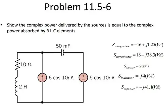
9

Summary / Question

I have this PCB (top only):

There is essentially no "signalling" happening here, and the only divergences from steady-state are when the input AC (T1) turns on or off, or when the right pair of pins of T3 are shorted (causing the relay K1 to engage and latch). State changes can be assumed to be separated by seconds, at minimum. See below for schematic and more information.

For the bottom, however, there are two obvious options.

  • I could just run traces:

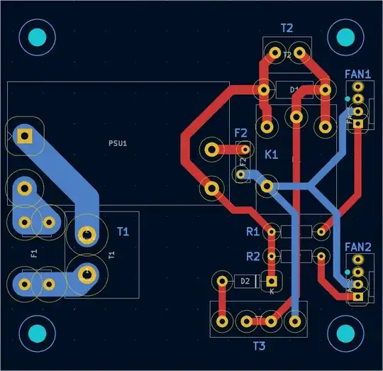
  • Or I could pour a voltage plane:

In a "non-signalling" application such as this, what are the advantages and disadvantages of each of these approaches? (Or are they both dumb? What should I be doing instead?) Also, in the pour case, should I be maximizing the size of the pour (keeping in mind it can't be "the whole board" in order to stay far away from the high-voltage AC), or keeping it closer to the convex hull of pads to which it connects?

Details

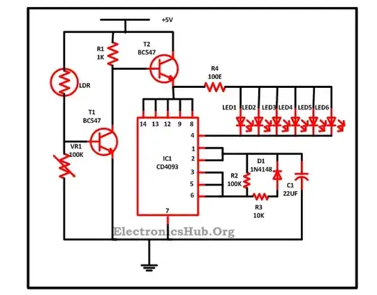
This is a manual delay-start circuit. Here's the schematic:

schematic

(Pin assignments for T1, T2 and T3 are arbitrary and may be switched in the PCB as compared to the schematic based on whatever works best for the PCB layout.)

Main switching happens upstream on the AC side. The intended functions of this circuit are:

  • Don't supply power to T2 until the user presses an additional button.
  • Keep power to T2 shut off if power from T1 is interrupted.
  • Illuminate an indicator when the T2 has power.
  • Provide power (stepped down by R1, R2) to some fans.

On the PCB, the very left is the AC mains input and can mostly be ignored, aside from "keep clear of this area". The middle top also needs to be unpopulated (and may even turn into a cut-out) for mechanical reasons.

For the left ("switched") and middle (ground) nets, I am very deliberately shaping the path from both the (inductive) load and relay coils to go directly to D2 before going anywhere else, as D2's reason-to-exist is obviously to 'eat' voltage spikes from these when the power goes out. For that reason, and because of the several nets on top, I don't really want to try to fiddle with pours on top.

Please use chat for any questions or suggestions not related to the pour-or-traces question.

Matthew
  • 481
  • 2
  • 12
  • as there appear to be no electrical considerations, the PCB manufacturer will use less etchant and have to dispose of less copper (so the job should be cheaper), if everything that can be is poured - so everything except a top and bottom isolation channel between LV and HV sections. – Neil_UK Feb 15 '23 at 06:50
  • 1
    @Neil_UK realistically I think they charge the same no matter how much copper is removed. – user253751 Feb 15 '23 at 13:20

3 Answers3

8

The answer, as with many things, is: "it depends."

Some reasons to create copper fills/planes:

  • You need a reference plane (often ground, but can be a voltage supply) for signals on an adjacent layer.

  • You need a low impedance voltage source, and/or delivery to multiple areas of a PCB, where a plane may offer advantages over routing traces.

    This seems most applicable to your specific case. You could use something like NEC EMIStream (an Altium extension) to analyze power and current to determine if traces are adequate, but it's quite a bit of effort if you're new to it.

    Although I can't determine if you would benefit from a copper fill providing the voltage source, I would probably not have the top-layer trace (red in your image) leave and return over the edge of the voltage polygon. This is sort of a split-plane crossing issue, and might result in noise because a signal is changing impedance at the crossing point. You mentioned that there are no high-speed signals here, but it's worth mentioning that the interval of the signal change ("separated by seconds") isn't the speed in question so much as the rising or falling edge of those transitions.

  • You have sensitive inputs on your device and need extra shielding, such as from RF interference. An example of this would be an antenna feed where ground pours would be used with via fencing.

  • Depending on design and materials, it may be desirable to utilize copper pours to reduce the amount of copper etching required. This is not very common.

Some reasons not to create copper fill:

  • Signals can inductively couple into no-net copper areas, and even couple onto adjacent traces simply by having an intermediate no-net copper area, properly grounding such islands with stitching vias becomes necessary to reduce crosstalk.

    Eric Bogatin has a particularly good explanation of this topic in his Altium Academy video "You Must Unlearn What You Have Learned." Look for the section titled "Copper Pour After Routing" that begins at 40:15.

  • Capacitive coupling can occur whenever a trace with changing potentials is coupled to a plane. It's complicated! See Power Plane and Ground Planes: Should You Use Your PCB Power Plane as a Return Path?.

There's an Altium Academy video in which Zach Peterson addresses your very question: "To Pour or Not to Pour | Copper Pour in PCB Design". There are also links to the following Altium articles:

Some of this isn't quite addressing your specific case, but my goal was to address the question title, "To pour, or not to pour? (And why?)" more broadly.

JYelton
  • 32,302
  • 33
  • 134
  • 249
  • "it depends"... which is why I asked for pros and cons and not just an answer. "My goal was to address the question [...] more broadly", which is the sort of answer I want. – Matthew Feb 14 '23 at 23:19
  • 2
    I've also heard that uneven distribution of copper can cause warping, though I think it's no longer a concern with modern manufacturing processes? – user253751 Feb 14 '23 at 23:22
  • @user253751 Indeed, the last article cites Lee Ritchey as saying that while omitting fills does reduce the amount of etching required, it is a trivial matter that doesn't really affect the PCB. It doesn't specifically address warping, so that may be a question for one's PCB fabricator. – JYelton Feb 14 '23 at 23:26
  • @user253751 I will add that I recently inquired about doing a 6-layer board with 1 oz copper except the bottom layer would be 2 oz, and the fabricator indicated that would require us to change our "warpage acceptance level from 0.75% (according to IPC standard) to 2% to 3%." I can see how a mostly-copper layer and a mostly-etched layer might contribute to warping in some cases. – JYelton Feb 14 '23 at 23:31
  • Right; warping is one of the points that probably deserves a mention. Is warping an issue with two-layer boards, though? I know it's something to do with epoxy and cooling, but... does that apply to a two-layer board? I thought the only layers after copper were solder-mask and silkscreen. – Matthew Feb 14 '23 at 23:42
  • 1
    @Matthew Yes it affects 2-layer boards as well, but how much depends on core thickness and what dielectric is being used. With "typical" FR4 1.6 mm boards it generally is of least concern. Your fabricator should be able to give you an idea of how much (worst case) to expect. – JYelton Feb 15 '23 at 00:10
5

I don't think it makes much difference one way or the other, assuming all your traces are generously sized for the currents involved. Parts that dissipate power would likely run somewhat cooler with the pour. You have provided good clearance for the pour so manufacturability will be pretty much unaffected if you use it.

You have some fast-ish edges on the relay coil (AM radio band roughly) as it scoots up to the TVS breakdown voltages and coupling that to the ground rather then distributing it as EMI may be not be advantageous (an argument for leaving the pour out, if that's not clear).


On an unrelated note, I would probably use the footprint for the form C relay as a talisman (prophylactic?) against availability issues for the form A relay, although the way it is laid out now you could just cut the lead off.

Also I would have put the traces on the bottom, which aids reparability and inspection (like if a misconnection blows a trace off). In that case the pour would be inconvenient in fitting a form C relay (probably require fish paper or something like that).

Spehro Pefhany
  • 376,485
  • 21
  • 320
  • 842
  • I am confused by the discussion of form B vs. form C relays. If you were talking about SPST vs SPDT, that would make sense, but the top search results say that the difference is NC vs. NO? I can't use an NC for this application, so I'm not sure what you're suggesting? – Matthew Feb 14 '23 at 23:28
  • Ah, my mistake Form A vs. Form C. – Spehro Pefhany Feb 14 '23 at 23:34
  • Ah, right. So, SPST(NO) vs SPDT. – Matthew Feb 14 '23 at 23:38
  • 1
    Yup, allow for the back contact if present. – Spehro Pefhany Feb 14 '23 at 23:41
  • If this was your board, and with respect to your argument against, would you consider a trace for the load/relay with a pour only under the fan lines (per jpa's answer)? Or do you disagree with the comment there on EMI from the fans? – Matthew Feb 15 '23 at 22:57
2

What are the advantages and disadvantages of each of these approaches?

Advantages of the ground pour:

1. Reduced inductance of current loops and thus less emitted EMI noise from any currents going through the board.

For example the fans will probably have some high frequency ripple in their current waveform. Anywhere where the supply and return conductors have distance between them, that ripple converts to a magnetic field that can couple elsewhere. The groundplane acts as a return conductor right underneath the positive wire, minimizing loop area. And for other current loops where neither conductor is ground, it still acts like a shorted transformer secondary, cancelling part of the magnetic field.

2. Safest place for any stray voltages to jump to

If there would be a lightning hit to mains wiring, and current jumps between the insulation gap, the ground plane is often the safest place where it can end up. At least it has a good chance for the rest of the circuit to survive.

Similarly, when a user touches your board, any ESD sparks would go to nearest metal surface. While this PCB does not have anything sensitive, one of the boards connected by cables could have and would usually survive better if the spike is to ground and not an IO pin.

3. Easily observable insulation distance

If your ground plane goes further than any of the traces, it is easy to check the insulation distance. For example, a certification engineer will want to measure the actual distance as manufactured and not rely on CAD drawings alone.

It also acts as a visual hint for anyone modifying the board design to "not go further than this". Same can be achieved with silkscreen lines, but a ground plane does the duty as well.

Disadvantages:

1. It takes up the second layer

If you had a lot of signals to route and really needed the second layer, any ground pour would be just a bunch of isolated areas and wouldn't do any good. At that point, you can just leave it off.

2. It increases stray capacitances

All traces going over the ground plane will have some capacitive coupling to it. In this case this is not an issue at all. For example medical electronics have maximum capacitance limits to avoid leakage currents to patients. But even there, the solution is usually extra shielding rather than removing ground plane.

jpa
  • 6,804
  • 17
  • 32
  • Okay... I've heard the thing about "return path" a lot, but... how does that work if the V+ and V- pins are very far apart? – Matthew Feb 15 '23 at 15:46
  • @Matthew If the far-apart pins are connected to cables, the cables will have a large loop area and will radiate no matter what PCB layout you have. In that case one could add ferrites to reduce the noise present in the loop. – jpa Feb 15 '23 at 16:53
  • Why would cables have a large loop area? They're usually run as pairs, sometimes *twisted* pairs. But... ignore the cables. Say I have the above situation, where "something" is the input of an optocoupler, and ignore what's on the other side. Also, is there a difference between pouring + and having a trace for - vs. the other way around? – Matthew Feb 15 '23 at 16:59
  • @Matthew If the individual wires from the cable are connected to pins far apart, the wires need to be separated. I don't understand the optocoupler question. Regarding what voltage to connect the pour to: it should be a stable voltage (to avoid emitting capacitively) and one of the conductors involved in critical currents in the design. In some opamp circuits V- or even V+ can be a fine choice instead of GND. In many other designs, the positive supply voltage may have some ripple that you don't want to couple capacitively to all other traces. – jpa Feb 15 '23 at 18:05
  • Sorry, I wasn't clear. Say I have some component (e.g. an optocoupler, or maybe a terminal that connects via twisted-pair wires to something else) that is the recipient of a signal. Say the *source* of that signal is pin 1 of a 30-pin IC (ahem, like an arduino nano board), but the signal needs to return to pin 16 (i.e. the pin furthest from pin 1). Does the current take the shortest path to pin 16, does it follow the trace from pin 1 until it just can't, or what? – Matthew Feb 15 '23 at 18:28
  • 1
    @Matthew For IC or a sub-PCB, any high-frequency components of the return current will follow the closest path they can get to the conductor inside the subassembly, because that path has the lowest high-frequency impedance. The current loop area will be relative to the vertical distance between the ground plane and the conductor in the subassembly. – jpa Feb 15 '23 at 19:15