4

schematic

simulate this circuit – Schematic created using CircuitLab

I came with this circuit to know how an active load can improve it, I still can't finish to understand the role of active loads. The far I know is that below, Q5-Q6-R2 form a current source with gives the polarization DC current to Q4. Then I expect the circuit would be similar to a common emiter, but as I suggested on the title I'd be thankful if someone could explain me (suppose the components are perfectly matched):

-What's the purpose of using an active load Q1-Q3-R1 instead of a single resistor on the collector of Q4 and what advantage gives

-What could be a possible application for this circuit

Thanks if someone answer

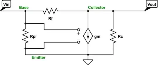
EDIT: Some research I did. Actually both upper and lower pairs are current sources and active loads. If they have the same reference current, they will polarize Q4 and the current on load will be 0. On the other hand, the AC circuit would be:

schematic

simulate this circuit

Since it must be that \$ V_E = g_m R_{EA} (V_{in} - V_E)\$, then:

$$ V_o = g_m (R_L//R_{CA}) v_{in} \left(1 - \frac{g_m R_{EA}}{1 + g_m R_{EA}} \right) $$

Where REA and RCA are the AC equivalent resistance of the AC model of the active loads. But they are function of frequency. And so, I looked carefully at the expression. Does this mean that the circuit could be a filter that dispenses with capacitors? I'm too drugged? What do you think?

tac
  • 335
  • 9
  • Do you plan to use this amplifier as standalone, or within more stages and a global feedback loop? – Designalog Feb 05 '23 at 07:28
  • But the configuration shows your circuit will act more like an attenuator than an amplifier. The gain will be less than one. We are adding an active load in the IC design to increase the voltage. And we cannot use the resistors because they take a lot of space in the silicon. Thus we use transistors instead as load. – G36 Feb 05 '23 at 08:15
  • But to get the benefits from the larger gain provided by an active load. Next stage input resistance also needs to be large. So this circuit is not suited to drive low resistance loads. And also some negative feedback is needed to "set" DC bias conditions at the desired and predictable "level". – G36 Feb 05 '23 at 08:24
  • 1
    This topology is basically not-working. You have two different current souces series connected, Q1 and Q5. Two current sources can't possibly drive exactly the same current and hence the operating point point can only collapse with one of the sources saturated. You should get rid of either Q1 or Q5. – carloc Feb 05 '23 at 08:28
  • @ErnestoG I don't know how to use this circuit. This is just an exercise given where one has to guess a possible application for the circuit – tac Feb 05 '23 at 15:56
  • @G36 but the active load requires the use of resistors R1 and R2 so you still need them – tac Feb 05 '23 at 15:57
  • @carloc ok but suppose the ideal conditions where all is perfectly matched. Actually I'm trying to find an application for this circuit, not to design, simulate or implement it – tac Feb 05 '23 at 15:59
  • But do you understand that now you have a circuit with no gain? \$Av \approx \frac{R_{CA}||R_L}{R_{EA}}\$ And REA will be large and it will depend on the collector current and on the Early voltage value REA = VA/Ic. Also, the two current sources are not needed. Only one current source at the collector will do the job. – G36 Feb 05 '23 at 16:21
  • @G36 I do understand that. Not all stages have to amplify voltage. Maybe if the active loads were not used, the AC resistance would be much lower and that would ruin the input and output impedance – tac Feb 05 '23 at 16:29
  • So what is your point? Or a problem? – G36 Feb 05 '23 at 16:34
  • @G36 What I mean is, maybe the input and output impedance would be somehow worse that what is needed here. My hypothesis is that the circuit just let pass high frequencies. Again I repeat: This is just an exercise given where one has to guess a possible application for the circuit – tac Feb 05 '23 at 16:37
  • As I said early the main reason why we add active load to the circuit is there is a desire to increase the voltage gain and to "remove" unwanted resistors from the integral circuit. – G36 Feb 05 '23 at 16:48
  • Related https://electronics.stackexchange.com/questions/450935/why-are-active-loads-used-for-transistor-amplifiers/507491#507491 – Sredni Vashtar Feb 05 '23 at 17:24

0 Answers0