How do we invent circuits?
In addition to revealing the idea behind this clever circuit, answering the question gave me the unique opportunity to show a somewhat little paradoxical way to invent electronic circuits by finding a useful application of a harmful phenomenon. I do this with the belief that no less important than the specific circuit explanations is to develop skills in how to understand, explain and invent circuits.
Basic idea
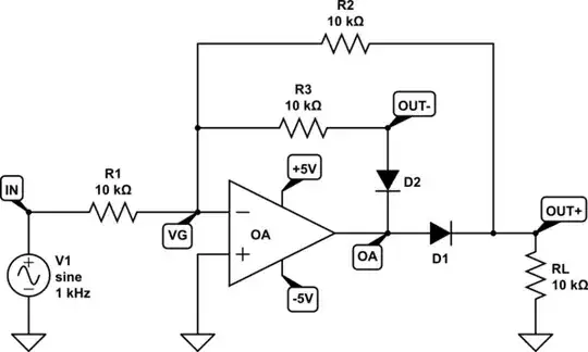
Inverting amplifier viewpoint
The circuit can be considered as an inverting amplifier in which the negative feedback network is split into two parts - one (D1-R2) operating during the negative input half-waves and the other (D2-R3) during the positive half-waves. The switching of the two parts is done with the help of the diodes D1 and D2. The two output signals are taken after the diodes; therefore the unwanted forward voltage drops across them are compensated by the op-amp.
The role of virtual ground
Thus, the circuit has two outputs - one for the positive output half-waves and the other for the negative half-waves... and we use one of them, in this case the positive one. Quite rightly, the question arises, "And what the hell is the second output after we do not use it?"
The role of this part of the negative feedback network is to maintain the virtual ground at the inverting input during the negative input half waves. If it were not there would be no virtual ground and the input signal would be transferred through resistors R1 and R2 to the circuit output (V2)... the feedback would become "feedforward":-)
The op-amp function
It is the same as our role in life when we realize our goals.
Op-amp follower. So, although this is a complex negative feedback circuit, the op-amp work is very simple - by varying its output voltage, it keeps the inverting input voltage equal to the non-inverting input voltage (zero); this is known as the "golden rule" of H&H. In this sense, any op-amp circuit with negative feedback is a follower where the voltage of the non-inverting input is the input and the voltage of the inverting input is the output. The simplest way to make such a follower is to connect the op-amp output to its inverting input. Then the op-amp will do its job without any effort.
Disturbed follower. But when the op-amp encounters obstacles (voltage drops across diodes and resistors), it starts increasing its output voltage more than usual in order to compensate for these disturbances. And as strange as it sounds, the primary disturbance is the external input voltage Vin... but it is a useful "disturbance".
D1 forward voltage is an undesired disturbance here; that is why, the output is taken after it and the disturbance is eliminated. The voltage divider R1-R2 is a useful "disturbance"; so the output is taken before it.
Implementation
STEP 1: Perfect half wave rectifier
simulate this circuit – Schematic created using CircuitLab
Zero input voltage. The op-amp effortlessly maintains zero voltage at its inverting input since no currents flow, no disturbing voltages; therefore its output voltage is zero... it just idles.
Negative input voltage. In keeping with our negative feedback philosophy above, this voltage change is a "disturbance" for the op-amp which it must eliminate. In the first instant, the op-amp fails to respond (as we do in life) and its output voltage is zero. The negative input voltage is transferred through the resistor R1 to the inverting input. The op-amp senses this change and begins to compensate by increasing its output voltage in a positive direction. With an excess of 0.7 V, it compensates the D1 forward voltage drop and starts passing current through the circuit R2 -> R1 -> Vin with the idea of restoring zero voltage to the virtual ground. Figuratively speaking, R2 acts as a pull-up resistor ("pulled up" by the op-amp) and R1 as a pull-down resistor ("pulled down" by Vin).
Positive input voltage. Now, the op-amp senses a positive change at the inverting input ("disturbance") and begins to compensate by increasing its output voltage in a negative direction. With an excess of 0.7 V, it compensates the D2 forward voltage drop and starts sinking current through the circuit Vin -> R1 -> R3 to restore the zero voltage of the virtual ground. Now R3 acts as a pull-down resistor and R1 as a pull-up resistor.
And here is the role of the negative feedback in this case - the virtual ground does not allow the transfer of the input voltage through the circuit R1 -> R2 to the load (more precisely, the op amp prevents this by drawing current from that point).
STEP 2: Imperfect half wave rectifier
The best way to convince ourselves of the need for a second negative feedback network is to see what happens if we remove it. Let's do it.
simulate this circuit
Only the case with a positive input voltage is of interest. Now the diode D1 is off and the op-amp can do nothing - it reaches the negative supply rail voltage and "stops". The input voltage is freely transmitted through the R1 -> R2 circuit to the load. A resistive voltage divider is formed and 1/3 of the input voltage is applied to the load.
STEP 3: Unloaded half wave rectifier
Apparently the load is the reason for this, we think; then let's remove it! But it gets even worse - now all the input voltage is passed to the circuit output!
simulate this circuit
STEP 4: Perfect full wave rectifier
And here we realize that we most often need a full-wave rectifier... and somehow, it worked itself out (I myself realized this idea a month ago when I answered a similar question).
It remains only to include a voltage follower (OA2) between the circuit and the load.
simulate this circuit
STEP 5: Deriving another principle
What have we done here? We have found a useful application of a harmful circuit phenomenon. This is a very powerful principle for solving inventive problems that can help us in other cases as well.
More examples of this principle are the use of the "harmful" voltage drop across a forward-biased diode as a useful voltage (e.g., in bias circuits)... or the "harmful" voltage drop across a resistor (current-to-voltage converter), capacitor (integrator), etc.


