\$3.3\:\text{V}\$ is not a lot to work with in a single stage like this one. Especially when keeping the output relatively undistorted while also providing an appreciable output swing. It's not complicated to see why.
The \$V_{_\text{BE}}\$ changes at the rate of about \$-2\:\text{mV}\$ per Kelvin. So an operating range from \$-20^\circ\:\text{C}\$ to \$55^\circ\:\text{C}\$ means a variation span of about \$\pm 80\:\text{mV}\$ around the quiescent point. Different BJTs will have different ranges. But this is a reasoned approximation.
So this suggests that the emitter voltage should be at least 10 times this, or about \$800\:\text{mV}\$ so as to reduce this impact to around 10%, or so. Already, this is eating into the tiny \$3.3\:\text{V}\$ rail.
The BJT itself should be kept well into its active mode. This means that the minimum magnitude of \$V_{_\text{CE}}\$ should be no smaller than \$1\:\text{V}\$. That's another chunk out of the tiny \$3.3\:\text{V}\$ rail.
From the above the maximum gain will be \$A_v=V_{_\text{E}}\frac{V_{_\text{CC}}-V_{_\text{CE}}}{V_{_\text{E}}^2-V_{_{\text{I}_\text{PK}}}^2}\$. So, if \$V_{_\text{EQ}}\approx 800\:\text{mV}\$ and given the input peak, perhaps a maximum \$A_v\approx 2.9\$. (This discounts the signal variation.)
Lowering things so that \$V_{_\text{EQ}}\approx 400\:\text{mV}\$, because of the small margins available, then the maximum \$A_v\approx 5.8\$. But then it is more temperature sensitive (and signal sensitive -- which means more distortion.) I'd recommend a lower voltage gain to be safer.
So, let's assume \$A_v=4\$ and \$V_{_\text{EQ}}= 400\:\text{mV}\$ and \$I_{_\text{CQ}}=1\:\text{mA}\$ and \$V_{_{\text{BE}_\text{Q}}}=670\:\text{mV}\$ with \$\beta=100\$. And that the base divider should be stiff enough that it presents about 10% of the collector current.
Then \$R_{_\text{E}}=R_4=396\:\Omega\$, \$R_{_\text{C}}=R_3=1.688\:\text{k}\Omega\$, \$R_1=20.273\:\text{k}\Omega\$, and \$R_2=10.7\:\text{k}\Omega\$.
Using standard values, say: \$R_{_\text{E}}=R_4=390\:\Omega\$, \$R_{_\text{C}}=R_3=1.8\:\text{k}\Omega\$, \$R_1=22\:\text{k}\Omega\$, and \$R_2=10\:\text{k}\Omega\$.
The result is, over temperatures from \$-20^\circ\:\text{C}\$ to \$55^\circ\:\text{C}\$:
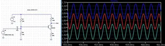
The gain is very close to prediction. And the variation over temperature keeps the collector voltage sufficiently high to work well in this situation. Also, \$\pm 80\:\text{mV}\$ against the emitter setpoint of \$\pm 400\:\text{mV}\$ suggests perhaps a \$\pm 20\%\$ shift in the bias point. And that is close to the observation here.
None of this takes into account the source impedance nor the load that needs to be driven by the circuit. It's assumed that the output is unloaded and the input has zero impedance. This is never true. But it seems as though the problem is more abstract than realistic. So perhaps this helps.
Calculations
Given a quiescent current, \$I_{_{\text{C}_\text{Q}}}\$, and the emitter set point, \$V_{_{\text{E}_\text{Q}}}\$, it's pretty easy to work out the emitter resistor value as:
$$R_{_\text{E}}=\frac{V_{_{\text{E}_\text{Q}}}}{I_{_{\text{E}_\text{Q}}}}=\frac{V_{_{\text{E}_\text{Q}}}}{I_{_{\text{C}_\text{Q}}}\,\cdot\,\frac{\beta+1}{\beta}}$$
(The above assumes a single power supply rail and ground.)
Knowing the voltage gain, \$A_v\$, the collector resistor is very similar but needs to take into account \$r_e^{\:'}\$ (which can be also represented as the assumed thermal voltage, \$V_T\$.) So the equation is:
$$R_{_\text{C}}=A_v\cdot \frac{V_{_{\text{E}_\text{Q}}}+V_{_T}}{I_{_{\text{E}_\text{Q}}}}=A_v\cdot \frac{V_{_{\text{E}_\text{Q}}}+V_{_T}}{I_{_{\text{C}_\text{Q}}}\,\cdot\,\frac{\beta+1}{\beta}}=A_v\cdot\left(R_{_\text{E}}+r_e^{\:'}\right)$$
(The thermal voltage is usually taken to be about \$26\:\text{mV}\$ and is less important for larger values of \$V_{_{\text{E}_\text{Q}}}\$.)
The resistor pair used to bias the BJT requires another parameter -- the divider 'stiffness'. If it's not stiff enough then the voltage variation at the BJT base, due to signal-dependent base current changes applied to the Thevenin equivalent resistance, will become unacceptably large. If it is too stiff, then a lot of excess current is wasted and the input impedance may also get unacceptably low.
Unless the specific circumstance presents unique problems, the idea is to 'waste' about 10% of \$I_{_{\text{C}_\text{Q}}}\$ in the divider pair. Since the base current will only be about 1% (or less) of \$I_{_{\text{C}_\text{Q}}}\$ for small signal BJTs, it won't affect the Thevenin voltage of the divider pair much. (Watch out for some power BJTs, though.)
So, if the 'stiffness' as a percentage of \$I_{_{\text{C}_\text{Q}}}\$ is \$k\$ and where a recommended value would be \$k=0.1\$ then:
$$R_2=\frac{V_{_{\text{E}_\text{Q}}}+V_{_{\text{BE}_\text{Q}}}}{k\,\cdot\,I_{_{\text{C}_\text{Q}}}}$$
and,
$$R_1=\frac{V_{_\text{CC}}-V_{_{\text{E}_\text{Q}}}-V_{_{\text{BE}_\text{Q}}}}{\left(k+\frac1{\beta}\right)\,\cdot\,I_{_{\text{C}_\text{Q}}}}=\frac{\frac{V_{_\text{CC}}}{I_{_{\text{C}_\text{Q}}}}-k\cdot R_2}{k+\frac1{\beta}}$$
The value for \$V_{_{\text{BE}_\text{Q}}}\$ can be estimated from a datasheet or from a simulation.


