3

Please consider the simplified Class D output stage below. Depending on the half-bridge duty cycle, different output voltages (within the power supply range) can be applied to the load.

schematic

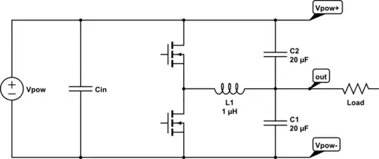
simulate this circuit – Schematic created using CircuitLab

The output filter is usually an LC filter like shown in the schematic. For all schematics that I have seen so far, the output capacitance is placed only in the position of C1, i.e. to the negative power rail. Now, for an application like a synchronous buck, that goes from 12 V to ~1 V that might be sensible because less bias will be present across C1 than across C2.

But when this topology is used to generate varying output voltages, both close to the positive or negative power rails (like e.g. in a Class D audio power stage), the DC bias of the output capacitors can change their effective value rather strongly for the case of usual X5R ceramics for example.

So I was wondering if one could distribute the output capacitance between C1 and C2 (i.e. to both power rails) to somewhat mitigate the effects of the DC bias on the total capacitance. Spice shows that the inductor ripple current nicely splits between both capacitors, so they are effectively in parallel for the ripple current. Is this a good practise to implement output capacitors ? It somehow doesn't look right to me.

tobalt
  • 18,646
  • 16
  • 73
  • 1
    Yes you can do this if you think that change in capacitance with a dc voltage change causes a significant loss of filter performance. – Andy aka Jan 16 '23 at 13:15

3 Answers3

2

Yes, and this might be better in certain technical aspects (startup transient, nonlinear capacitors), but less so in practical aspects such as EMI where the negative rail may be the reference plane. (I think it's more likely such a class-D amp has a common ground rail, which makes more sense in this regard.)

But EMI may be a small issue, as a subsequent LC filter could be applied against the reference plane, easily addressing RFI issues at least. (A filter stage at EMI frequencies probably affects the overall filter design, so can't just be tacked on, just something to keep in mind.)

Tim Williams
  • 22,874
  • 1
  • 20
  • 71
  • Indeed, the idea is that the halfbridge is floating, but the output will be RF-decoupled to an EMI-ground (there will be more filtering on the output) – tobalt Jan 16 '23 at 15:45
1

Assuming you'll have a PI filter in which the L has a non-zero DC resistance, with the split cap configuration there's going to be large peak currents (larger than the inductor current's peak) flowing through the caps during the rising and the falling of the bridge voltage (assuming the load is Vpow- referenced). The peak values depend on the rate of change (rising and falling). Since the difference of these currents is be equal to the inductor current, there won't be any peaks visible at the load side. However, depending on their values, these peaks may lead to a temperature rise for the caps which may result in extra capacitance decrease. And not to mention possible EMI issues. Slowing down the rate of change by adding some capacitance across the switches might be a solution but it's not always under the designer's control or it's not always possible or easy.

With single cap arrangement none of the issues mentioned above will be present.


The advantage is, as you mentioned, relatively higher effective capacitance. The DC bias of each cap will dynamically change so while one cap has lower capacitance the other will have higher. But the difference may not be that noticeable.

Here's an example:

Assume the supply voltage is 12V and two 1812-case 4.7u/25V (having the following graphs) are used for C1 and C2: enter image description here

If the duty cycle is 25%: For split cap arrangement, the voltages across the C1 and C2 will be 3V and 9V, respectively. At 3V C1 will be ~4.7u, and at 9V C2 will be 4.4u, so the effective capacitance will be 9.1u. If these caps were in parallel across the output, both of them would see 3V and the effective capacitance would be 4.7u x 2 = 9.4u.

If the duty cycle is 50%: Split cap and the other would bring equal effective capacitance.

If the duty cycle is 75%: Split cap arrangement would bring 9.1u while the other arrangement would bring 8.8u.

So the difference doesn't seem to be noticeable. However, in applications where the capacitor's voltage could be close to their rated voltages then the difference would be more noticeable. See what would the results be for 24V supply voltage.

To me, the benefit doesn't seem to be worth to make the layout a bit more complex.

Rohat Kılıç
  • 26,954
  • 3
  • 25
  • 67
  • It is for 48V nominal Vpow, so I'll have to check some of those C(VDC) curves carefully. Could you please explain why there would be switching related peak currents (more than in a only-C1 scenario) ? – tobalt Jan 16 '23 at 15:44
  • @tobalt For the supply you'll probably have a PI filter in which the L has a non-zero DC resistance *(I should've added this detail into my answer, sorry. Now I'm adding it.)*. Make an LTspice simulation and you'll see. If you won't have any filter then just ignore this. – Rohat Kılıç Jan 17 '23 at 08:04
  • Sorry for asking again. The load is indeed Vpow-referenced. Why would anyone ever use a pi-filter as output filter after a half-bridge ?? That first C in the pi filter (which I assume, you mean would be on the *left* side of L1) is just tremendous useless burden on the switching transistors. So no, I don't have a pi-filter, just the L right from the switch node output into the output caps. (Of course there might be very small snubbing components near the switch node itself). So I am still not really sure which current spikes you are talking about.. through *which* components ? – tobalt Jan 19 '23 at 07:38
  • @tobalt I wrote "For the **supply** you'll probably have a PI filter..." I meant supply filtering, I didn't say anything output filtering. – Rohat Kılıç Jan 19 '23 at 07:42
  • Ok, so assume we have a pi filter after the Vpow source. Then through which components will there be a current spike when the half-bridge switches, and how will this current spike be higher/different compared to the situation where C2 is missing? – tobalt Jan 19 '23 at 08:09
  • @tobalt you have a simulation tool. Simulate it and see it yourself. – Rohat Kılıç Jan 19 '23 at 08:35
  • Rohat, I am asking (after 2 days) because I cannot reproduce this excess current in my sim (nor hypothetically in my mind), so obviously I have accidently done something wrong (such as failed to include some crucial parasitic effect). I guess what you may mean: When the transistors switch and demand current from the power rail, it usually comes from the input cap. With the split cap arrangement, it will *also* take some of it from the output caps (but accordingly *less* from the input cap). Is that what you mean ? – tobalt Jan 19 '23 at 08:52
  • 1
    @tobalt partially. Have a look at [this](https://wetransfer.com/downloads/524e1f5d87d1e90f0de90e5a4b95c5ff20230119103227/6517efb9a707be9d94bd6291daedf8c220230119103423/976003). – Rohat Kılıç Jan 19 '23 at 10:37
1

I have done this with caps in 1995 .This was before Spice simulation being common .My application had 3 470microfarad old school phillips 037 35VDC eltec caps .Input voltage was 24 and 12 VDC out. Hence duty cycle was about 50% . No reliability issues or emc problems .Now younger engineers have simulated this with no suprises.

Autistic
  • 14,235
  • 2
  • 27
  • 65
  • Do you mean, that you had put 1) one cap as the input cap, 2) one cap as the output cap to the positive rail and 3) one cap as output cap to the negative rail? Have you ever run such a converter *without* the input capacitor? After all, the input capacitor becomes (somewhat) redundant when both C1 and C2 are present?! – tobalt Aug 31 '23 at 07:37
  • @tobalt .I did use an input cap as well ,so yes 3 identical caps .Well you could consider no input cap and maybe 25 volt caps ,yes cheaper but ripple current and available parts in the day meant that i did not do this. – Autistic Aug 31 '23 at 08:10