3

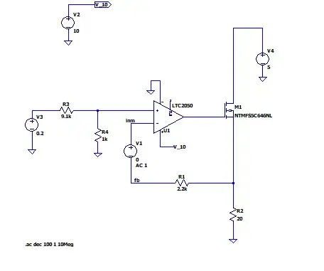
Short summary: V3 decides the current going through R2. If V3 is 0 V then no current is going through R2. If V3 is 10 V, it will be approximately 50 mA.

I want to do an open-loop simulation of this voltage-controlled current source.

Transient

The conventional method is to remove the DC current source (V3) and add a small signal analysis source at the feedback, and do an AC analysis frequency sweep of V(fb)/V(inm).

open_loop_simulation

Nothing useful can be found using this simulation method. You need a DC operating point at the non-inverting input of LTC2050 (U1) for it to drive the nMOSFET gate (M1.) It seems like the minimum DC-operating point is 0.2 V.

I ended up with this simulation, and also a reasonable Bode plot:

open_loop_simulation_2

phase_margin

The phase margin for this circuit is 56°, with a DC operating point (V3) of 0.2 V.

Now comes my question:
Should I simulate this open-loop simulation with different DC operating points or just select the minimum DC operating point? V3 will have a voltage that varies from 0 V to 10 V.
ocrdu
  • 8,705
  • 21
  • 30
  • 42
Tungstein
  • 47
  • 5
  • *Should I simulate this open-loop simulation with different DC operating points?* <-- what do you hope to achieve? What is the point of this exercise? Is someone telling you that simulations are needed? – Andy aka Jan 15 '23 at 11:49
  • Previously I designed this voltage-controlled current source with a different nMOSFET with a larger input capacitance, and unfortunately it was oscillating. – Tungstein Jan 15 '23 at 12:00
  • It takes less than a minute to simulate a particular scenario and ten minutes to simulate ten different scenarios and, what I'm saying is that I don't know why you are asking this question because, it takes so little effort and time to do any number of simulations. Spend an hour or two simulating as many different scenarios as you can is my advice. – Andy aka Jan 15 '23 at 12:11
  • I asked this question because I was not completely sure if I was actually doing a proper open-loop simulation when you have a DC-operating point, and I was not sure if I should set different DC operating points while doing an open-loop simulation. – Tungstein Jan 15 '23 at 12:23

3 Answers3

3

A comment under the question by the OP: -

I asked this question because I was not completely sure if I was actually doing a proper open-loop simulation when you have a DC-operating point, and I was not sure if I should set different DC operating points while doing an open-loop simulation.

You might just as well do a bunch of closed-loop simulations with a step change on the input and look for a problematic sustained overshoot in the voltage across R2. This would indicate things are potentially going to go a little unstable.

I'm not a massive fan of open-loop simulation tests because, they can miss-the-point --> it's got to work closed-loop hence, look for instability with a step change on the input demand.

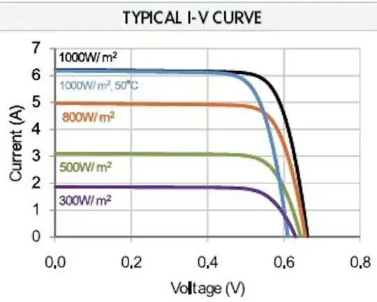
Try changing the input demand from say 1 volt to 3 volts and look at the voltage change dynamically on the source pin of the MOSFET. The following picture was taken from a site dealing with servos and instability but, it's exactly the same with the op-amp because it's a control system but operating in microseconds rather than seconds or milliseconds: -

enter image description here

You can expect some undamped overshoot and ringing from a step-change but, if there is a sustained ringing seen on the output then, the closed-loop response is getting close to full instability and you might need to apply a small capacitor from op-amp output to its inverting input.

You can also do an AC response in closed-loop to see if there are any unforeseen peaks in the spectrum. Again, this would apply an AC signal at your input (biased to about the mid range) and look for excessive spectral peaks at the MOSFET source.

Andy aka
  • 434,556
  • 28
  • 351
  • 777
  • I did try using a a small capacitor from the op-amp output to its inverting input, and it removed alot of the oscillation, but the phase-margin was so poor in the original nMOSFET that it did not remove the oscillation entirely. **Again, this would apply an AC signal at your input (biased to about the mid range) and look for excessive spectral at the source.** Do you mean the non-inverting input? And then measure over the source of the mosfet? And by excessive spectrals you mean spikes? – Tungstein Jan 15 '23 at 13:07
  • Use your actual input for this. No need to try and inject anything anywhere else @Tungstein. Then look at the MOSFET source. I've modified that sentence to make it more obvious. – Andy aka Jan 15 '23 at 13:28
  • Okay, cheers mate. I think I have enough tools in my tool box now to be certain that in the next revision there will be no oscillation. – Tungstein Jan 15 '23 at 13:38
  • OK @Tungstein good luck and, if you get a step output waveform that might show too much ringing (indicating poor phase margin) then please show it if you need more advice. – Andy aka Jan 15 '23 at 13:44
2

You're probably outside the input common-mode range of your amplifier when you test your current source with a 0V input. Perhaps you should have some negative voltage supply as well to accommodate this.

I think it's a good idea to simulate with different input voltages. Perhaps exploring the extremes (0 and 10V) is a first good test of your stability.

What's the function of R1? You're doing a current source. Somehow you're also setting the voltage amplification at the R2 top node. IMHO, I think you should remove it.

Designalog
  • 3,232
  • 1
  • 13
  • 23
  • The function of R1 was to have the same input bias current at the non-inverting and inverting input of the op amp. So R1 shall be equivalent to R3 || R4. However the values are wrong in the simulations. – Tungstein Jan 15 '23 at 12:20
  • Please, do the calculations and check whether you're actually doing what you are intending to. What I see is you forcing a voltage gain of 1+R1/R2 at the source of the NMOS. Is that what you intended as well? – Designalog Jan 15 '23 at 12:26
  • 1
    No, the intention was not to have a voltage gain of 1 + R1/R2. Indeed, I shall probably consider removing the feedback resistor. – Tungstein Jan 15 '23 at 12:59
1

As suggested in the comments, I made a simulation that shows (a little) the "change" of margins.

Phase & Gain margins shown are for V3 = 1 V.
Opamp is an old LF13741 Open Loop Gain=75-85 dB).

enter image description here

enter image description here

Antonio51
  • 11,004
  • 1
  • 7
  • 20
  • Are you doing a closed-loop simulation where V3 is frequency sweeped? – Tungstein Jan 15 '23 at 13:47
  • No. It is open-loop analysis through the tool "probe" of microcap v12. V3 is used as a parameter for setting DC bias. One can see that the OL gain is "little" affected except in the case of V3 = 0 (don't know why). – Antonio51 Jan 15 '23 at 14:09