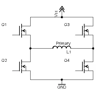
The eval board for the GaN half bridge module LMG5200 (datasheet) contains the following circuit to generate dead time from a single PWM input.
The half-bridge module itself has good propagation delay matching (2 ns) and fast switching (few ns). Therefore, the eval board advertises that a short 7.7 ns dead time is sufficient.
My question is, isn't this circuit unsuitable to generate the dead time for such a fast half-bridge? Wouldn't the dead time be strongly different between the UP/DOWN transitions? Because the LO_SIGNAL branch contains one additional LVC inverter (U3C) with a propagation delay of nominally 5.4 ns.
Is this skew somehow compensated? If not what could be used as a more symmetric dead-time generation circuit from a single PWM input? One version I have found mentioned a lot uses a delay and two gates (AND, NOR) (example from Andy). But I wonder, if it is appropriate for ~ns delay matching because it uses two different gates.

