0

I found a 500W inverter implementation with an Arduino Nano and IR2101. According to its schematic, I think the input connections of both IR2101 are wrong. If it is wrong, then why is this circuit is working fine in the video? Did I get it wrong?

Video: 500W Sine Wave Inverter Using Arduino - H Bridge

Schematic, PCB and program: ElectroMux- 500W sine wave inverter with auto voltage
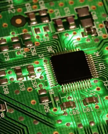
Schematic

Deepak
  • 5
  • 2
  • 4
    Why do you think that is wrong? How do you think it should be? – Justme Dec 28 '22 at 22:06
  • 1
    Looks fine to me -- what do you think is wrong with it? – TimWescott Dec 28 '22 at 22:07
  • Because both inputs of IR2101 get the same PWM pulse and thus both FETs turn on at the same time which is a shoot-through situation. – Deepak Dec 28 '22 at 22:17
  • The HIN and LIN both inputs of IR2101 must never both be high at the same time, that's why we need dead-time. Here is both FETs from half-bridge of one side are connected to the same input pulse, both turn on at the same time, and the same is true for other half-bridge. Am I getting it wrong? – Deepak Dec 28 '22 at 22:39
  • 2
    I think you are correct. The LO1 and LO2 should be swapped so that the high side of one leg turns on with the low side of the other. An IR2104 has a single PWM input and should work as shown. – PStechPaul Dec 28 '22 at 23:17
  • 1
    , but I also think those 10k resistors on the gate are too high, a quick look at the datasheet suggests 30nC charge on the gate at 12V, so you're looking at about 100us risetime with the 10k resistor. – Bryan Dec 28 '22 at 23:40
  • 1
    Tracing the simple PCB layout provided shows that it matches the schematic shown above, and the video seems to show the same board but with some components changed (such as gate resistors are 47 ohm). The Arduino sketch seems to show only two pins being alternately driven with PWM. So something is "fishy" ;) – PStechPaul Dec 29 '22 at 23:38
  • 1
    Also, the video shows a low battery protection function, but the Arduino sketch does not implement that, nor does the schematic show it. – PStechPaul Dec 29 '22 at 23:54

2 Answers2

4

There are a few things to comment on this circuit:

  1. First-off, the bootstrap capacitors \$C_1\$ and \$C_2\$ are way of too high a value. Remember that these caps are refueled when the low-side transistors \$Q_2\$ and \$C_4\$ are turned on. So brutally applying a low-impedance 12-V dc source across a capacitor generates a high current spike and must be avoided. You even may collapse the 12-V source. Therefore, I would recommend you reduce these caps to around 0.1 µF, a low-voltage film type will do well (25 V). Their value depends on the driven \$Q_G\$ but 100 nF is a fairly standard value.

  2. Add a small 10-Ω resistance in series with the bootstrap diodes \$D_1\$ and \$D_2\$. This is to limit the above current spike in the bootstrap capacitors. Even with 100 nF, there are spikes which are sources of disturbance and must be limited.

  3. Add 47-kΩ resistors across the gate-source of each MOSFET (closely located to the pins). This is to keep the transistors off in case you have a bad connection or a dry solder joint. No need to go too low for this resistance as it consumes a bit of driving current.

  4. Reduce the gate series resistance to a lower value, something like 10 to 47 Ω, also very closely located to the gate. These resistances are there to damp the \$LC\$ network made of the MOSFET input capacitance and all the inductive traces brought by the PCB. They can resonate and must be damped. They also slow-down the turn-on transition and limit the \$t_{rr}\$-related losses in hard-switching situations.

  5. When working on the control pattern for the MOSFETs, add some dead-time between the upper- and lower-side transistors. Either by software or with a simple circuit like in here. This is to avoid shoot-through currents (the transistors conduct together for a small amount of time while actuating them and it creates spikes and power dissipation).

  6. Before sending the switching pattern with the Arduino, turn \$Q_2\$ and \$C_4\$ on alone for 1 ms or so. This is to pre-charge the bootstrap capacitors at 12 V and thus have the driver \$V_{cc}\$ ready before sending the full pattern. It will avoid the first erratic pulses linked to a supply voltage close to the twilight zone for the driver, e.g. the UVLO level : )

  7. I read the comments on the drive inputs of the half-bridge drivers and they can't obviously be connected together and need separate signals, hence the comment in bullet 5.

The circuit given in the ZIP looks fairly simplistic to me. I recommend you assemble the power section without any transformer first and supply it from a low-voltage, current-limited source that you slowly raise while observing the drive and output signals. Good luck with this project!

Verbal Kint
  • 20,420
  • 1
  • 16
  • 50
  • 1
    Thanks for all your clarifications. If I assemble it, I don't think it will work with the current configuration. We can see that this would lead to a shoot-through situation. It works fine (still questionable) if we swap LO1 and LO2 as suggested by [@PStechPaul](https://electronics.stackexchange.com/questions/647972/driving-h-bridge-with-ir2101#comment1719891_647972) , and it's working in the video because the creator updated his implementation with the correct configuration, but forgot to update the schematic and PCB layout files, maybe. – Deepak Dec 29 '22 at 16:46
  • 1
    @winny, thank you for turning ohms into \$\Omega\$ but I brought the hyphens back : ) The hyphen is there to form a compound adjective: "the capacitor is 10 µF but I replaced it by a 22-µF type" or "the current is 3 mA but I measured a 10-mA leakage current", "a 12-V source" etc. Believe me, I have learned it the hard way with all my papers/articles : ) Thank you for your kind help! – Verbal Kint Dec 29 '22 at 17:10
  • @VerbalKint I see your point on the value itself versus the “name” being referred to. – winny Dec 29 '22 at 18:34
0

Be carefull with this schema, the value of the elements are not right, on other schema has been published for a 1000w inverter and for example the IR2101 pin 1 and 4 are not connected and the bootstrap is wrongenter image description here

it's from the same author

rollins
  • 1
  • 1
  • The author is designing faulty circuits but still they are working fine. – Deepak Dec 29 '22 at 19:13
  • 1
    There's a lot wrong or missing in that second schematic and it looks like maybe it is for driving a push-pull center tapped transformer to get 220 VAC. It's certainly not what is in the video, which shows four MOSFETs with 47 ohm gate resistors and 100 uF bootstrap capacitors. The circuit seems to work OK in the video, so it;s a shame that it's not properly documented. – PStechPaul Dec 29 '22 at 22:55
  • Hello. yes it is, but also I can't understand why this project has been published. have also seen an other project with push_pull driver with a couple of bd140 and bd139 witch look more reliable for an inverter with 7-0-7 V transformer. – rollins Dec 30 '22 at 12:34