4

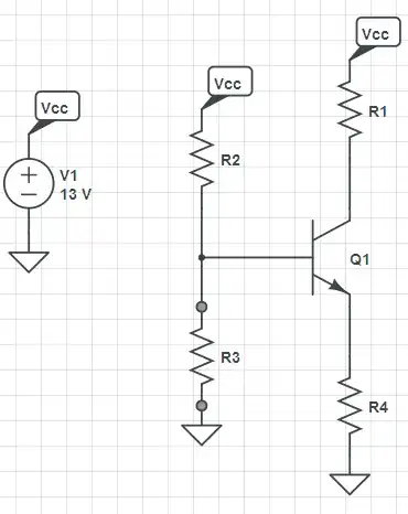
I'm to the task to design a BJT Common-Emitter Amplifier with resistance at the emitter as in the figure, and for that I need to:

  • get the values for \$R_{1}\$, \$R_{2}\$, \$R_{C}\$ and \$R_{E}\$
  • given \$I_{CQ} = 3\text{mA}\$ , \$V_{CEQ} = 6.5\text{V}\$ ,\$V_{CC}=13\text{V}\$ and \$\beta = 380\$ for a BC547C transistor.

Currently I'm able to analyze correctly the circuit given the resistances, but the reverse process, that is, getting the resistances values given only the operating point is what is giving me problems as there is various "rules of thumb" and considerations to make, I'm trying to use the "1/3 rule of thumb" (\$V_{E} = V_{C} = V_{CE}= V_{CC}/3\$) but I'm not getting the expected results \$V_{CE}\$ since \$V_{CE}\$ is already given.

How can I go to design this circuit?

enter image description here

jippie
  • 33,033
  • 16
  • 93
  • 160
favner85
  • 83
  • 2
  • 6
  • 1
    For a common emitter, R4 should equal 0\$\Omega\$, the circuit is more stable with a higher resistor value but it is no longer called Common Emitter. – jippie Apr 07 '13 at 19:05
  • I meant to say a common-emitter with a resistance at the emitter. Edited the original question. – favner85 Apr 07 '13 at 19:10
  • It is just as much a Common-Base with a base resistor ... or a Common-Collector with a collector resistor. – jippie Apr 07 '13 at 19:13
  • Is the total gain of the circuit known? – jippie Apr 07 '13 at 19:16
  • You know the \$V_{CE}=6.5\text{V}\$ and \$V_{CC}=13\text{V}\$, so the rest of the voltage is across R1 and R4. With \$\beta =380\$ you can assume \$I_C\$ and \$I_E\$ are equal. \$I_C\$ is given, so you can calculate the sum of the two resistors. If you know the total gain, then you can calculate R1 and R4. – jippie Apr 07 '13 at 19:21
  • Also you know \$I_C\$ and \$\beta\$, therefore you know \$I_B\$. – jippie Apr 07 '13 at 19:24
  • No, only the stated data. Seems there are a lot of variables to consider. Trial and error is time consuming and not so much of engineering approach. – favner85 Apr 07 '13 at 19:25
  • If you know the gain, you can solve the whole circuit, in that case you can calculate the ratio for R1 and R4. Then all the voltages are known. Choose current through R2+R3 to be at least 10 times \$I_B\$. – jippie Apr 07 '13 at 19:25
  • The gain is not known beforehand. I was thinking if we could get what \$V_{E}\$ is it would be much easier, here comes the said assumptions several authors make, what is a 'correct' values for \$V_{E}\$ ? – favner85 Apr 07 '13 at 19:30
  • \$V_E\$ depends on the gain. Now if your requirement is maximum output swing on the collector (which would make sense because \$V_{CE} = V_{CC}/2\$, then again R4 equals 0. In that case you can solve the circuit too I guess as all voltages are known in that case. – jippie Apr 07 '13 at 19:38
  • 1
    Join us in chat: http://chat.stackexchange.com/rooms/15/electrical-engineering – jippie Apr 07 '13 at 19:38
  • This problem is under-specified. There is more than one way to pick the resistor values such that the given \$V_{CE}\$ as well as quiescent current are achieved. – Kaz Apr 08 '13 at 07:38

3 Answers3

2

We are not here to do your homework for you, so I'll just give a broad approach. Ask specific questions if you get stuck on any individual point.

  1. Decide the gain you want. I wouldn't try to make a single stage produce more than 10x voltage gain for most normal applications.

  2. The gain dictates the ratio of R1 / R4.

  3. Decide the max current you can afford to have this draw.

  4. At the lowest output, figure you want to keep 1/2 volt on the transistor. That means the max current from step 3 will be (Vcc - 1/2 V) / (R1 + R4). That gives you absolute values for R1 and R4.

  5. Find the collector voltage at the maximum current operating point from the previous step. That will be your lowest output voltage. This highest will be Vcc when there is no current thru the transistor. Try to bias the transistor so that the collector volatage will be close 1/2 way between these two extremes.

  6. Determine the voltage to hold the base at to achieve the collector bias point.

  7. Find the worst and best case base currents for the bias point, using the min/max assumptions about the transistor's gain.

  8. Design the R2-R3 voltage divider to produce that voltage using a mid value for base current. Check what happens at the base current extremes. If the collector voltage varies too much, then your circuit is too dependent on the transistor gain and you need to adjust something or relax some specs.

Show the values you picked. For extra credit, tell us the resulting input and output impedance of the amplifier.

Olin Lathrop
  • 310,974
  • 36
  • 428
  • 915
1

If i were designing this amplifier I'd want Ve to be as low as possible but not zero volts. Linearizing the BE current for ac input voltages is a must for low distortion amplification unless there is feedback from collector to base (and there isn't).

Actually there is feedback and that is caused by the emitter resistor BUT don't make it too big because the output voltage undistorted p-p swing will be reduced.

So it's a trade-off and I'd consider making Ve about 0.5V.

That will then tell you how to calculate R1 and R4 (because you know the desired collector current). Knowing the quiescent collector voltage is 6.5V is not a big deal because almost certainly, in this type of academic question it's Vcc/2.

If you didn't have a target collector current delivered in the question you'd have to reckon it out yourself by analysing what load would connect to the amplifier and what frequency response (high frequencies) you needed to attain for the desired performance.

You have Beta and from that you can calculate the base resistors, but, don't try and use all the beta - use about a third or a half. I tend to use 0.6V as the forward volt drop of the base which means there is 0.5 (Ve) + 0.6 (Vbe) volts on the base.

BTW, rightly or wrongly I'd call it a common emitter circuit if the output is at the collector and this type of circuit almost certainly would be in that category.

Andy aka
  • 434,556
  • 28
  • 351
  • 777
1

By using the following approach I was able to solve my question:

Let \$V_{E}=1/10 V_{CC}\$ and \$R_{BB}=(1/10)betha*R_{E}\$ where \$R_{BB}\$ is the Thevenin's resistance.

\$V_{E} = 13/10 = 1.3V\$ so \$R_{E} = V_{E}/I_{E} = V_{E}/I_{CQ} = 1.3V/3[mA]\$ given that \$I_{C} >> I_{B}\$

Which yields \$R_{E}=433[Ohms]\$

\$R_{C} = (V_{CC} - V_{CEQ} -V_{E} ) / I_{CQ} \$ resulting in \$R_{C} = 1.73[kOhms]\$

\$R_{B} = (1/10)*380*433 = 16.454[kOmhs]\$

Thevenin's Voltage:

\$V_{BB} = I_{CQ}((R_{BB}/betha) + R_{E}) + V_{BE}\$

\$V_{BB} = 2.21289[V] \$

From the voltage divider at \$R_{2}\$:

\$ V_{BB} = (R_{1}*V_{CC})/(R_{1} + R_{2}) \$

\$R_{2} = R_{B}*V_{CC}/V_{BB} = 100.47[kOhms]\$

From the thevenin's resistance:

\$ R_{1} = R_{BB} / (1 - (V_{BB}/V_{CC})) = 19.64[kOmhs]\$

Resistors values which satisfies the target Q point.

favner85
  • 83
  • 2
  • 6