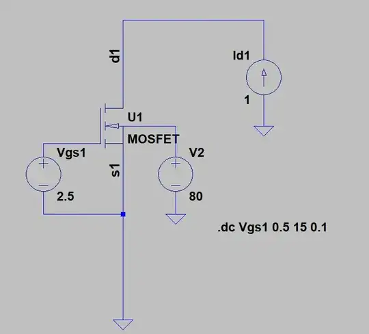
I don't see anywhere any .model so I have to conclude that you're using the basic 4 pin NMOS, which has no such thing as temperature pin. The 4th pin is the bulk and, typically, it's tied to its lowest potential (source here). So, what you did was you forced the bulk to be at a higher potential than the drain. Thank goodness that SPICE has no magic smoke (or is it?). But, if you are using a custom model or subcircuit, please let me know.
Then, you are plotting Vd/Id which, in the first two cases there is a difference of a resistor between them. It's one thing to plot Rds, and another Rds+R.
The third method uses a current source and, as you know, it will deliver that current no matter what. It will also force a different operating point through sheer will.
So, if you want to know the Rds you'll have to first take care of the operating point. The usual way of doing this is with the usual curves which, at its most basic setup, is with two voltage sources:

Two things to note:
- I am carelessly using the voltage at the bulk greater than the potential at the source -- this is gross but, it's there for the sake of exemplification
- In real life test cases the sources will have a limited impedance and there will be some resistors added, to avoid high currents.
Also, the test is revolving around the threshold voltage, which is set through the .model at vt0=2.5. That's where the sharp change happens so that's where the focus is (and given that, in your pictures, you seem to be interested in the transition).
