2

I am designing an SMD PCB to control two motors that consume 6 amperes each. I have too many components and I am using 4 layers, but it is very disorganized, so I want to separate the tracks.

I want to know how to separate those tracks, and in which layers can I put the signals power, the signals control and the differents signals in the board.

I have found information about the power signals must be in a internal layer but the power signals in my circuit need a wide track (5 mm) so I put it in an external layer, is that ok? Do I need a ground plane or power plane?

My circuits specs are: One ESP32 for control the H bridges of the motors

  • Two H bridge with N-channel MOSFETs
  • Two current sensors
  • Two ADC converters
  • Two voltage regulators (3.3V,5V)
  • Four weight sensors

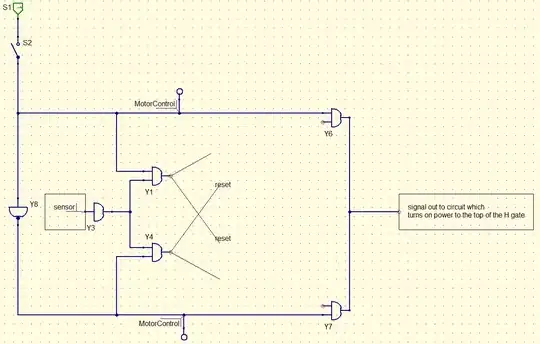
The connection of signals power in my circuit:
enter image description here

enter image description here

JRE
  • 67,678
  • 8
  • 104
  • 179
  • 2
    Put high current tracks on the outer layers with no resist or silk screen over them, then you can beef them up by soldering a thick copper wire onto the surface if needed. – Neil_UK Dec 13 '22 at 08:14

2 Answers2

2

There are not strict rueles but some general ones on how to organize your layers that come from years of experience. You are free to put any track on whatever layer you want.

  • In a four layer board the inner layers are used for power supply (area fill)
    • One GND layer (can have several area fills or wide tracks for example to separate AGND and DGND or Power GND)
    • One power layer where the power supply or power supplies to the different paert of the board are routed. Can be done with fills or wide tracks.
  • Outer layers
    • separate the tracks by direction to make routing easier. Like "Top layer mostly vertical and bottom layer mostly horizontal"
    • tracks that have high current on the outer layers so they can get rid of the heat easier (the need to be wider on the inner layers)

Other best practices:

  • Make your life easier for testing / measuring
    • don't put vias in pads if you can avoid it.
    • try to make every signal accessible from the top (don't route a signal directly under an IC and put it to an inner layer via a via)
    • prefereably, every signal should be accessible from the top layer (accessing signals with a probe from the bottom is a payn except if you're using a needle adapter)
    • label your testpoints (preferably with good names, but at least number them)
    • put testpoints on every signal (if constrained for space you can leave out the ones on THD components because there you can contact the leads with a probe easily)
    • use trough hole testpoints if possible (they are easier to put the tip of a probe into and solder a wire to to connect something)
  • Tracks as wide as possible (except for impedance controled lines)
  • Check the pad sizes of your footprints, they are often way too small (for handsoldering use oblong pads)
  • for high current, calculate the track withs. 1mm (40mil) is good enough for 3A on outer layers and 1.5A on innel layers (temperature rise < 20K). KiCAD has some nice calculation tools for stuff like that.
  • Spend time on cleaning up the text on the silkscreen before sending the board off to the manufacturer
    • put thexts in the right place
    • uniform with and height (where possible)
    • only text that are of use
    • all thext that is of use
    • put an article umnber / description / revision on your board
  • Mark your layers (TOP, BOT in copper as text)
  • Put an easy to check dimension on the fab layer

that's an incomplete list but that's what I just had in my head...

kruemi
  • 2,994
  • 16
  • 29
1

A Power or Ground layer should separate the power tracks from signal tracks prone to cross-talk. These are coupled by caps to decouple local current surges. If there is a thermal rise from this then chances are great high dI/dt may cause EMI problems.

If they get hot but and have high dI/dt then EMI and heat are two contentious issues. If high dV/dt then buried between Pwr and ground would be better for EMI but worse for thermal rise as the FR4 is a thermal insulator.

Since you have made these tracks very wide, you may have used the free Saturn PCB Design tool to compute the thermal rise, impedance, and C of the tracks already.

The layout of distributed 12V & Gnd current and risetime are important factors, which are why some designers use busbars for Pwr and gnd if they want to avoid dedicated layers of pwr & gnd.

Tony Stewart EE75
  • 1
  • 3
  • 54
  • 182