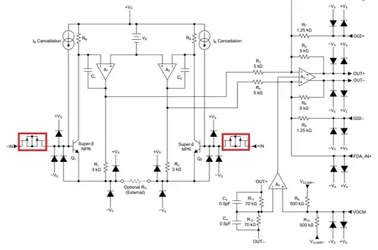
I was looking at the INA851 and trying to understand the input over-voltage protection. I can't seem to figure out what this pictured part is.
3 Answers
It's part of the input port over-voltage protection on the INA851. Basically it acts as a current limiter should excessive over-voltage occur: -
So, a constant current diode (a real device) is made from an N-channel JFET and resistor like this: -
Because it will conduct as hard as it can in the "wrong" direction, two are used (back-to-back) in series: -
And, depending on the construction of the JFET, the resistor can be internal hence: -
And, of course they can be made from P-channel devices equally well (as the INA851 circuit indicates): -
- 434,556
- 28
- 351
- 777
It looks like it's two depletion-mode FETs tied back-to-back. If I'm reading the purpose of that correctly, it should look like a series resistor under normal circumstances, but source or draw a constant current to or from the input transistor base when the input voltage gets excessive.
So, basically, it looks like it's a protection circuit.
- 44,867
- 1
- 41
- 104
