2

enter image description here

enter image description here

enter image description here

Dear all, I have simulated an AND gate in LT Spice which uses discrete method as shown in the diagrams. However, when V18 is 4V and V17 is 0V, I still get 1V at the output (orange colour) which the real voltage is suppose to be 0. May I know how to solve this issue :)?

jessica smith
  • 521
  • 1
  • 10
  • With this gate design, you can't. This is not a good AND gate. – Hearth Nov 23 '22 at 16:14
  • Make R33 lower in value like 1 kohm but you still won't get 0 volts so reduce your expectations is my advice. – Andy aka Nov 23 '22 at 16:49
  • Jessica, see [this recent answer](https://electronics.stackexchange.com/a/641992/38098). In it, near the top, I include another link. And it carries another pair of links. Use them all. What you have is a crappy example used for teaching an idea but failing to use a practical circuit for same. So it is only good when speaking to the public about an idea. It's not good to actually use it. – jonk Nov 23 '22 at 17:47

3 Answers3

3

I still get 1V at the output (orange colour) which the real voltage is suppose to be 0.

That's a normal BJT behaviour.

Remember an NPN BJT's diode representation:

schematic

simulate this circuit – Schematic created using CircuitLab

What you have done is to forward bias B-E junction with 4V through 10k and 4k7. So the biasing current is:

$$ V_{18}=V_{BE}+I_b(4.7\cdot 10^3 + 10 \cdot 10^3) \\ \Rightarrow I_b =\frac{4-0.6}{14.7} \mathrm{mA} = 0.23 \mathrm{mA} $$

Since there's no voltage at the collector, the transistor won't do any current amplification.

The B-E junction bias current will flow through the resistors and finally, drop around 1V across a 4k7 resistor.

This is a principal AND gate design, and requires some modifications for practical applications. You can start with increasing the base resistor (R35) to decrease the biasing current. This will drop less voltage across R33. But still, you won't be able to get exactly zero volts. Think about a BJT-inverter (NOT) followed by a BJT NAND gate.

EDIT: I think I should "circuitise" my suggestions above.

Making a BJT-NAND and an inverter (NOT) will bring better results:

schematic

simulate this circuit

With the circuit above, the outputs will be taken at supply-voltage levels. The optional, marked area is to make the output impedance low. The circuit can still work as expected even without that section, but the output impedance will be around 4k7, which is relatively high, when the output is taken from Q3. So, when it comes to cascade different blocks/gates, having a low-output-impedance driver is beneficial or can be even necessary.

Rohat Kılıç
  • 26,954
  • 3
  • 25
  • 67
  • Hi sir, so how do you make it to 0V on my LT SPice circuit? What modifications must I make? – jessica smith Nov 23 '22 at 16:18
  • 1
    @jessicasmith As I said above, you can't. This is not a good design for an AND gate. NAND works better; use that followed by an inverter. – Hearth Nov 23 '22 at 16:23
  • I designed an NAND gate followed by AND gate using discrete components in LT SPice but I still could not get any positive results. I updated my post above – jessica smith Nov 23 '22 at 16:32
  • Hi, you said that this is a bad design, may I know what are some of the good designs of AND gate using 2n2222 transistors? Can you show some :) ? – jessica smith Nov 23 '22 at 16:45
  • @jessicasmith A good design would be a NAND gate followed by an inverter. Takes one more transistor if you're using RTL logic like this, but gives you proper output drive and both inputs are equivalent. This is how AND gates are usually (but not always!) implemented in logic ICs like the 74xx series (though that's TTL, not RTL). – Hearth Nov 23 '22 at 16:49
  • Hi, what if I do not want to purchase those chips? I want to build the entire and gate using discrete component which is 2n2222 :)? – jessica smith Nov 23 '22 at 16:51
  • @jessicasmith You can make the same circuit outside of an IC. I'm just using it as an example--this is what the internals of a 74-series NAND gate look like. There's no rule saying you can't make it out of discrete parts. – Hearth Nov 23 '22 at 16:53
  • @Hearth, hi, I could not find the internal circuit for the NAND gate in the 74-series on the web. Do you mind sharing a diagram in your answer :) ? – jessica smith Nov 23 '22 at 17:21
  • @jessicasmith Search for "BJT nand gate" and "BJT not gate". Put them together and you'll get something like this: https://i.stack.imgur.com/rZQwF.png – Ste Kulov Nov 23 '22 at 17:32
2

Hi, what if I do not want to purchase those chips? I want to build the entire and gate using discrete component which is 2n2222

I provided a simplified example of designing for a 5 V RTL gate. Please refer to it for details.

I dislike the 'supposed' BJT AND gate that looks like this topology:

enter image description here

If you see one like that, again. just realize it is nearly useless except for a hand-waving education.

A more usefully direct answer would be this:

schematic

simulate this circuit – Schematic created using CircuitLab

That only uses 2N2222 NPN devices. And you can chain these together where the outputs can handle up to six attached inputs. However, the output can sink a lot more current than it can source.

jonk
  • 77,059
  • 6
  • 73
  • 185
1

Here's a simple design that guarantees virtually zero (I think zero with seven decimals places before 45 nano volt).

When either input is zero (not both of them 3 V), the output is for all practical purposes zero (< 1 uV).

The PNP transistor in the middle is the trick because it's completely cut off when either of the inputs to the AND Gate isn't High - when either transistor is cutoff, the Base current of the PNP transistor has not outlet, forcing the PNP to be off as well. When the PNP is off, there is not current to the Base of the rightmost Emitter Follower. With no current, that transistor is also cutoff, such that no current flows through the rightmost 5k load resistor.

Since the rightmost 5k load resistor is at the output of an Emitter Follower (its load resistor), it can be reduced (or increased) quite arbitrarily.

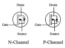
Each of the Gates Activate at about 1.7 V (or higher, 3 V in the image below is more than enough), while keeping off below 1.7 V (I'd give it a bit of a buffer and say below 1.2 V to ensure an off gate).

The NPN transistors can be 2N3904 or 2N2222 (2N3904 is better except for very high power applications). The PNP can be 2N3906.

I highly recommend the Falstad simulator because LTSpice is not as helpful for educational purposes (in my view), because it's not animated and not "real time". For anything DC, the difference between Falstad to LTSpice might be in the millivolts.

enter image description here

enter image description here

enter image description here

LTSpice results (the UI is harder to use in my view and at least in my case I was never able to leverage it to really learn something that I didn't already know from before):

3 V one gate, 0 V another gate (closer to zero than Falstad, in the pV rather than nV):

enter image description here

Both gates high (3V) - 30 mV difference with Falstad, but it's 30 out of 8310 (less than 0.5%):

enter image description here

Edit: Rohat Kılıç's Tomem pole idea for the last stage output is very nice too (instead of an Emitter Follower). Upside: you get 8.9 V instead of 8.3 V when ON. Downside: you get 115 mV instead of 0 V when OFF.

Depends if the 0 V or the high voltage is more important to you. I learned something, because never thought of totem poles in the context of digital outputs.

enter image description here

ee_student
  • 447
  • 1
  • 2
  • 8
  • The problem with taking the output from an emitter follower is that the logic-high voltage can never be at supply level i.e. will always be a Vbe lower. Using totem pole output is the way. – Rohat Kılıç Nov 24 '22 at 07:31
  • very true if you're concerned about losing 0.7 V from 9 V for the High voltage level.. – ee_student Nov 24 '22 at 07:33