Continue tracing the circuit. Look up datasheets and design notes. PSUs rarely stray far from the recommended application, little point in doing so.
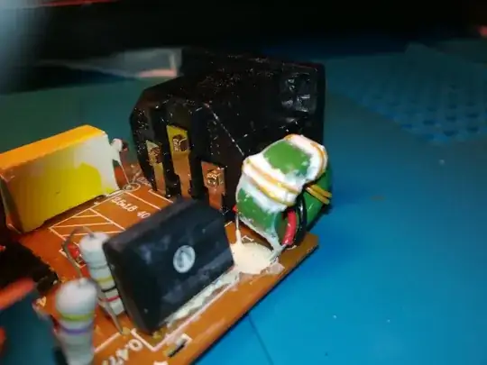
CMC looks woefully insufficient, I wonder what levels that thing actually met. The green core could be anything, but if it's a CMC it better be a hi-mu (>8k?) ferrite. The yellow wire is probably TIW, hence no need for large separation (>3mm) to meet a mains voltage rating. Given \$\mu_r\$, ID, OD and height, the \$A_L\$ of the core can be calculated, or it can be looked up among similar parts.
That's 4 turns, by the way. Count the number of passes through the center. Even a bead-on-lead arrangement still counts as one turn -- the current has to loop back around somewhere, somehow!
The transformer will be some standard flyback arrangement, air gap in the middle, modest \$A_L\$. Looks like a PQ or ER something type? Take dimensions and look it up, Ae and le being the most important figures. mu isn't too important, it'll be some ~2k material, cheap and effective. Knowing operating frequency and power level, peak current is known, and estimating core losses, \$A_L\$ and gap length can be estimated.
Turns ratio can be measured by excitation (apply say 5V 100kHz to primary, measure others). Also check leakage by shorting other windings and measuring primary inductance again.
Edit:
Yikes, the creepage distance on that thing...
Namely, the clearance between primary and secondary sides, particularly around the opto. Maybe this was intended to run LEDs or something? Something that can't be touched, so doesn't need much if any isolation?
Normally, some 8mm or so is required between primary and secondary, for the output to be touch safe (SELV as defined in e.g. UL/IEC 60950-1, and superseding standards).
The zener is unusual, but seems to serve as overvoltage limiting (pulls up current sense, making it turn off earlier and thus throttle down, when Vaux is too high).
The "470pF?" between Isense and Vfb is surely erroneous; I wonder what that's about. (Not necessarily that I doubt your tracing; mind, this unit doesn't appear to be a very well-designed example..!)
Typically a 1k series resistor, and 470pF shunting to GND, is applied to Isense, to give some noise immunity -- mainly to reduce the turn-on transient, when the transistor's gate capacitance is charged, plus transformer winding capacitance. More advanced controllers integrate this as a function, "leading edge blanking", usually ignoring the pin entirely for the first say 200ns after turn-on. An RC filter serves a similar purpose, but costs the two components.
The other thing it could be, is 470pF across the VFB or COMP pins, maybe to tweak compensation. (Compensation is mostly secondary side via TL431 (or similar) error amp; the controller is basically wired as a constant current source, which the secondary side controls to maintain desired output voltage.) But returning this to Isense doesn't make any sense either.
The feedback path seems to be missing some things. There's no pull-up or down for the phototransistor to drop voltage into.
Normally, a pull resistor is used to make a reference voltage, which either overrides the COMP pin directly (commonly done, but poor design: the pin current range is poorly defined, so who knows how much opto current is required to override it?), or the error amp is wired as an inverting buffer (e.g. 10k resistor from opto to VFB, 10k from VFB to COMP) from it.
Here, it seems they need VFB to pull up by its own bias current (which it should: datasheet says 0.1-2µA out of the pin), and then the opto can pull it as low as 2.5V by shunting towards COMP. Which does not, however, actually cut off the controller -- COMP needs to go below ~1.2V to do that. (Maybe that's why they put in the zener, to keep it from blowing up at light load?)
Finally, the opto seems to be backwards. VFB will pull higher than COMP, putting C-E negative. This, I think, still works, as it's a photodiode mode instead (photocurrent isn't amplified by transistor action; or, maybe it still is, but at inverted hFE? -- which is generally lower than in forward mode). But, as there's no bias resistor in parallel with the opto LED, the TL431 won't be able to draw any bias current without also turning on the phototransistor; and even in photodiode mode, those ~µA will be drawn quite quickly (i.e. with maybe less than a mA of LED current).
Finally, output doesn't seem to be well filtered. The two electrolytics will have quite some ripple left over (fractional volt?). This would be fine for some applications, but likely blows out emissions for any typical load, and probably isn't too nice in the first place, in terms of interference sent to whatever's connected. Aside from very basic loads like lights.
Along with the woefully insufficient CMC, it does seem emissions was... not a priority of the designers here.
