When the circuit is in steady state, a capacitor can be replaced by an open. However, I have seen an example where a capacitor was used in place of a resistor in a negative feedback loop, and the condition that the input voltages were equal was used in solving for the output voltage of the op-amp. How is this possible?
Asked
Active
Viewed 720 times
2
-
6Do you have more context (and a schematic) for that example? Was it analyzing the behavior of an op amp when exposed to high-frequency signals? Nothing so far seems like a contradiction, but it's difficult to write up an answer without having the context. – nanofarad Nov 10 '22 at 18:48
-
Probably using complex-valued AC analysis. – Jonathan S. Nov 10 '22 at 18:49
4 Answers
3
I really like this question, in spite of its brevity and lack of context. It shows that at least you've identified issues with capacitive feedback and quiescent state.
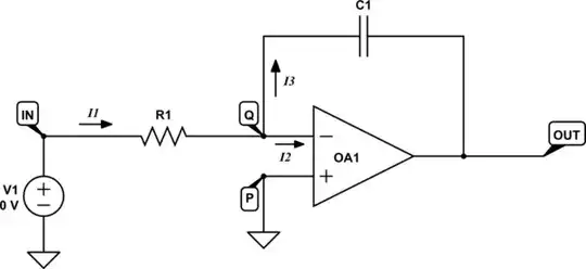
Start with the classic op-amp integrator circuit, assuming that all components and conditions are ideal:
simulate this circuit – Schematic created using CircuitLab
If this were a perfectly ideal operational amplifier, and the capacitor had no idiosyncrasies that might complicate matters, and that there's no such thing as noise, then behaviour is really easy to explain. Start with the fact that C1 provides negative feedback, which has the effect of causing the op-amp to adjust its output potential to whatever value is necessary to equalise the potentials at its inputs Q and P, \$V_Q = V_P = 0V\$.
Secondly, the op-amp input draws no current, so by KCL and Ohm's law:
$$ I_3 = I_1 = \frac{V_{IN}}{R_1} $$
Then there's the relationship between current \$I_3\$ through C1 and the voltage across C1 \$V_{C1} = V_Q-V_{OUT}\$:
$$ I_3 = C_1 \frac{dV_{C1}}{dt} $$
which translates to a few interesting behavioral facts:
If \$I_3\$ is constant and non-zero, the voltage across it will change at a constant rate (in volts-per-second), a rate proportional to \$I_3\$. Since node Q is held at a virtual-ground, zero volts, \$V_{OUT}\$ is what changes, and where you will see this "integrating" behaviour.
There will be an accumulation over time of charge on C1 (and the corresponding voltage across it), if the input potential \$V_{IN}\$ is even the tiniest bit non-zero. This is usually very problematic, because it's super difficult to produce conditions that result in exactly zero quiescent current through C1.
If \$I_3\$ can be maintained at exactly zero, the output potential stays where it is, which is not necessarily zero.
In reality of course there are input offset voltages, input bias currents, and all manner of imperfections that complicate matters, but the fact remains, if you can establish a condition at IN that results in no current flowing via R1 through C1, then \$V_{OUT}\$ will remain steady, unchanging.
Under those conditions, with all imperfections accounted for, with no further perturbations in temperature, input voltage or anything, and \$I_3 = 0\$, then since no current is flowing through capacitor C1, it's no longer playing any role in this "quiescent state ", and it can be removed without influencing anything. Conditions would remain as they are even if you repeatedly removed and re-inserted C1, or even replaced it with a cell of exactly the same potential difference.
However to return to the vague context of your question, what is the probability that the DC operating point of the entire circuit that contains this module provides exactly the right potential \$V_{IN}\$, to push exactly the right current through R1, that will be exactly the right amount to bias the op-amp input so that \$V_P - V_Q\$ multiplied by some ridiculously large open-loop gain produces a conveniently small \$V_{OUT}\$, well within the op-amp's power supply potentials (i.e without saturating the op-amp output)? I would say that probability is vanishingly small.
In other words, this integrator circuit is not really suitable for DC operating point analysis, except in the context of ideal components and conditions. If indeed you were to remove C1, to establish the quiescent state of the circuit, and if you were to account for all imperfections of the op-amp, such as input offset voltage, output voltage limits and so on, you'd probably find the op-amp to be saturated before you even start transient analysis.
You are right to ask this question, and I think you can give yourself a pat on the back for identifying the absurd idea that this circuit has any such thing as a "steady state". It does not. Without C1 in place the op-amp is open-loop, and all bets are off. You are at the mercy of any variance in the op-amp's parameters from device to device. Without feedback, it is now a digital comparator, not a linear amplifier.
Even with C1 in place, the integrating nature of the circuit means that the output is always changing, unless you can establish \$I_3 = 0\$ somehow during your DC operating point analysis. Steady state here is very difficult to achieve.
The solution is usually to place a large resistance in parallel with C1, to slowly "bleed away" any charge accumulated, due to non-zero quiescent current through C1, and to provide a tiny amount of negative feedback at DC, bringing DC gain down to something more predictable and reasonable than 100,000 or a million, or whatever the op-amp has.
Simon Fitch
- 27,759
- 2
- 16
- 87
-
So under ideal conditions, in the quiescent state the input voltage difference can equal 0 only when Vin is 0. Then is there no difference between using a capacitor as negative feedback versus no feedback? – nova Nov 12 '22 at 20:24
-
@nova that is correct, though I reiterate that the condition for quiescence is that I3 be 0A, which in practice will *not* correspond to Vin being exactly zero. Close, but non-zero none-the-less. – Simon Fitch Nov 13 '22 at 03:49
2
Those circuits are incomplete. If it is an integrator you're talking about (or anything with capacitive feedback), then they'll normally take feedback resistor in parallel with that capacitor so that the input and output of the amplifiers are well-defined at DC.
I believe standard electronic books do not, usually, include the parallel feedback resistor into the schematic when introducing the circuit to a new student as it might clutter the concept and schematic itself... something I totally understand.
There are cases in which the resistors are not needed, but that's usually when the input and output nodes are defined at DC elsewhere. This happens, typically, when an integrator is used in the feedback loop (as a "DC servo").
Designalog
- 3,232
- 1
- 13
- 23
-
Provided the integrator *is within an overall DC feedback loop* (such as is often the case in voltage regulators), a resistor in the feedback loop of the error amplifier (which can also be the loop integrator) is not necessary. – Peter Smith Nov 11 '22 at 08:26
-
Indeed. I meant to say that with "input and output nodes are defined elsewhere". – Designalog Nov 11 '22 at 08:28
-
Another case when there is no need of parallel feedback resistor is if the capacitor is periodically discharged. – Circuit fantasist Dec 29 '22 at 07:17
0
These are my thoughts.
If you are solving for the DC operating point t->inf and you know that at t->inf the circuit goes to DC values and the AC goes away (sometimes with prior knowledge you can do this with visual inspection). The input must also not be changing.
If you know that it does go to a DC value at t->inf and you are solving for DC then the current through the capacitor must be zero at that time. You can then omit it from the DC analysis.
Voltage Spike
- 75,799
- 36
- 80
- 208
0
Although the moderators declared that this question needs details of clarity and, for this reason, the question is closed, the question title unambiguously defines the class of circuits so distinctly that you do not have to see the circuit drawing in order to fully appreciate the problem.
The question body discloses the context of the OP confusion that resulted in this question. That the OP accepted the meticulous answer that reiterates considerations of many textbooks and lecture notes containing basic math of the ideal op amp analysis at the beginner level, leaves no doubt that this derivation is what the OP sought, and they got it with the accepted answer.
Still, the question title is attracting the attention of visitors via internet searches, and, for the students at the more advanced level, it might be of interest that the opamp circuits with pure capacitive feedback exist and are very useful. @ErnestoG mentions one example in his answer, with @PeterSmith's apt comment. I am going to elaborate on this subject with a reference to the Renesas application note AN551 Recommended Test Procedures for Operational Amplifiers.
For visitor's convenience, I use here the circuit drawing and few excerpts from this document. The circuit is developed for the industry-accepted NULL method for operational amplifier testing used in mass production. I learnt of this circuit while looking for an answer to @kenearl's question What is the best way to simulate the open-loop gain of an op-amp in LTspice.
The circuit TEST CIRCUIT 1 from the Renesas application note 551, page 5

is used to measure offset voltage, input bias current, input offset current, common mode rejection ratio, and open loop gain.
When measuring the offset voltage, the gain of this circuit with RF = 50K (RF = 5M) requires the output to be driven to 1000 (100,000) times the offset voltage necessary to maintain the output of the AUT at 0V. Overall circuit stability is maintained by the adjustable feed-back capacitor \$C_A\$. Notice that this adjustable feed-back capacitor \$C_A\$ is the only component of the path connecting the BUFF opamp output and the BUFF inverting input, and this is the circuit of the topology class identified in the OP question title.
V.V.T
- 3,521
- 7
- 10