2

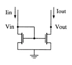
I'm trying to build an XOR gate following this schematic without any simplifications:

enter image description here

Here is the circuit itself:

enter image description here

T1 and T4 are inverting the signal (the NOT gates), T2/T3 and T5/T6 are the AND gates, and the circuit is missing the final OR gate because I got lost at this point.

The resistors connected to the push buttons are 120 kΩ, the ones connected to the transistors are 5 kΩ and the ones connected to the LEDS are 180 Ω.

When I built the upper half alone it worked as expected, pushing B (right button) turns the LED on because the low A (left button) is then reversed to high and the AND outputs high.

The lower half worked as expected too, except it's the opposite, so pushing A (left button) turns the LED on.

But when both are connected at the same time, neither of the LEDs turn on under any circumstances. When I test with a multimeter, the bases of T3 and T6 are at around -0.8 V, and when buttons are pushed they are at around 1.5 V, but again, the LEDs are not turned on the slightest.

Here is a schematic to display the connections, I hope it's not confusing:

enter image description here

The input source is 5 V.

ocrdu
  • 8,705
  • 21
  • 30
  • 42
  • 1
    possibly the parallel transistors aren't exactly identical so one has a lower Vbe, so the voltage goes down to that one's Vbe and the other doesn't turn on. What if you use a separate resistor per transistor? – user253751 Nov 10 '22 at 01:41
  • Actually all 6 of them are BC337 NPN transistors. For the left button, I moved the bottom red wire to a different pin and connected that pin to the button through a resistor, is that what you meant by separate resistor? If so, it still does the same thing. – Soufiane Touil Nov 10 '22 at 01:46
  • 2
    We normally draw schematics with the positive supply at the top, Ground or negative at the bottom, and arranged so the signal flows left to right - much easier to understand things that way. – Peter Bennett Nov 10 '22 at 01:53
  • Thanks for the tip @PeterBennett, I'll do ASAP – Soufiane Touil Nov 10 '22 at 01:58
  • 4
    @SoufianeTouil Even transistors with the same part number are not exactly identical. I mean a separate resistor for *each* transistor when they are in parallel. – user253751 Nov 10 '22 at 02:02
  • Inside your schematic, you have some overlapping nodes, which look connecte,d but according to your solver are not connected – Ferrybig Nov 10 '22 at 09:29
  • @user253751 Sorry, I'm confused a little, in my circuit above, don't I have 2 5K resistors connected to T1 and T4 separately? – Soufiane Touil Nov 10 '22 at 14:41
  • @Ferrybig I realize the schema is a mess, I'll redraw asap following Peter instructions. – Soufiane Touil Nov 10 '22 at 14:49

3 Answers3

4

Your two-transistor AND gate and output indicators are wired like this:

schematic

simulate this circuit – Schematic created using CircuitLab

This does not work because the LED will have current going through it if just B is a logic 1 regardless of what logic level A is at.

This thread on the EEVBlog:

https://www.eevblog.com/forum/projects/why-does-this-two-transistor-and-gate-not-work-as-expected/

suggests some alternatives such as:

enter image description here

and:

enter image description here

ErikR
  • 4,897
  • 11
  • 18
  • I assume the LED will turn on if only B is on because of the current from base to emitter, without the need of current from collector to emitter, am-I right? I believe due to the high 120k resistance in the base of the transistors, not enough current is passing to turn on the LED, making it "seem" like an AND gate, but it's really a cheap trick, correct? What's confusing me really is that many websites are showing the same schema for an and gate, what is the difference between the first schema and the one in this website: http://hyperphysics.phy-astr.gsu.edu/hbase/Electronic/trangate.html – Soufiane Touil Nov 10 '22 at 14:35
  • Interesting conversation at eevblog, apparently the 'and gate' schema that is being shared everywhere is wrong, it really makes sense. – Soufiane Touil Nov 10 '22 at 20:11
  • The Hyperphysics AND gate doesn't follow TTL rules for output voltage levels. If A is 0V and B is 5V the output is 1.38V which is in the forbidden region -- i.e. above the maximum for a logic low voltage and below the minimum for a logic high. – ErikR Nov 11 '22 at 04:47
  • The NAND and NOR gates on the Hyperphysics site work fine, but the AND and the OR gates have problems. – ErikR Nov 11 '22 at 05:12
  • The gates would likely work if MOSFETs were used instead of BJTs. – ErikR Nov 11 '22 at 05:20
4

When you are talking about small numbers of BJTs and larger numbers of resistors in order to make logic gates, you are talking about RTL -- resistor-transistor logic. There is a design process involved. I provide a simplified example of that process for a 5 V RTL gate. Regardless, you don't just shoot from the hip if you plan to stack gates together, safely and securely.

Specifications are important. I've borrowed a diagram from that earlier post I mentioned (on the topic on a \$5\:\text{V}\$ RTL gate):

enter image description here

Above, you can see what's considered to be a valid LOW and HIGH and the area where an input voltage would be considered INVALID. Each stage can source a valid output HIGH for up to 6 specified sinking inputs, which is the more difficult, limiting case. (Each stage can easily sink a valid output LOW for many more inputs.)

I will use both RTL inverters and RTL NORs to construct the XOR. I will also add a standard LED driver switch. Since the maximum sourcing from a standard gate is about \$\frac{5\:\text{V}-2\:\text{V}}{4.7\:\text{k}\Omega}\ge 400\:\mu\text{A}\$, I set the LED current for \$6\:\text{mA}\$ (assumed saturated \$\beta=15\$.) It should work if you build it:

schematic

simulate this circuit – Schematic created using CircuitLab

That's it. The way it works is to that \$Q_5\$ is a NOR gate, which takes as its inputs the outputs of two other NOR gates, \$Q_3\$ and \$Q_4\$. \$Q_3\$ just takes \$A\$ and \$B\$ as its inputs. But \$Q_4\$ takes \$\overline{A}\$ and \$\overline{B}\$ as its inputs. The circuit presents \$F=\overline{\overline{A+B} + \overline{\overline{A} + \overline{B}}}=\left(A+B\right)\cdot\left(\overline{A} + \overline{B}\right)=A\cdot\overline{B}+\overline{A}\cdot B\$. Which is an XOR.

I really hate the commonly found 'supposed' BJT AND gate that looks like this topology:

enter image description here

If you see one like that -- run, don't walk, away. It's nearly useless.

jonk
  • 77,059
  • 6
  • 73
  • 185
  • Perfect, it works like a charm! I have a couple of question though, what is the point of Q6 ? And would-you say that the schema in my original post would work with a correct AND gate and resistors values? Also, since the transistor gate is not specified though you did not refer to a datasheet and I just randomly picked BC337 and it worked, how did you come up with the resistor values? is it just experience? Thanks for the help! – Soufiane Touil Nov 12 '22 at 22:19
  • @SoufianeTouil In the link I provide in the very first paragraph, you can see the design steps. As for \$Q_6\$ it's just an LED driver. The gates themselves made up by \$Q_1\$ through \$Q_5\$ cannot directly source current into an LED, well. The max would be roughly \$500\:\mu\text{A}\$. That might be enough to see, especially if you have a high efficiency RED LED handy. If you do, just hook it up with anode to \$Q_5\$ collector and cathode to ground and get rid of the \$Q_6\$ circuit, entirely. But it will be very *dim* with a standard LED. Worth a try, though. – jonk Nov 12 '22 at 23:39
0

schematic

simulate this circuit – Schematic created using CircuitLab

How would these work for logic gates? They should be expandable to multiple inputs.

PStechPaul
  • 7,195
  • 1
  • 7
  • 23