Your circuit shows a glimpse of DC/DC controller similar to LM5146-Q1, so it seems quite natural to search TI's online documents for design examples where this type controllers are driving external power transistors having the Kelvin source pin. If the search gives no sensible results, the examination of designs with controllers for GaN FET transistors is useful, because GaN FET transistors also exploit Kelvin connection.
GaN FET power transistors in the circuit Simplified Typical Application, datasheet LMG1210 half-bridge MOSFET and GaN FET driver, page 1
have a Kelvin connection pin, although the connection is shown only for a low-side transistor. But the document TIDA-01634, Multi-MHz GaN Power Stage Reference Design for High-Speed DC/DC Converters shows both high-side and low-side power transistors with Kelvin connection pins connected to the gate driver IC.
The low-side transistor's Kelvin pin is connected to VSS, low-side ground return. There is no pin in LM5146 specific for low-side ground return; I think you can continue using PGND for this purpose, only take care of PCB wiring recommendations as given in the manufacturers' documents for low-loss switching designs. The high-side transistor's Kelvin pin is connected to HS, a switch node and high-side ground return, which is a functional analog of LM5146's pin SW: it is used to reference the internal high-side gate driver input against a true source voltage of the external high-side transistor having the Kelvin source pin. Notice that the circuit shows no direct connection between the high-side-transistor-power-source/low-side-transistor-drain node AND the controller.
However different might be the two controllers (LM5146-Q1 and LMG1210) in their implementation, the comparison of their functions supports the decision to connect the driver source pin of high-side power transistor to SW. To provide the advantage of lowering switching losses with the help of a Kelvin source pin, the internal gate driver of the controller should be given the true gate-source voltage not distorted by induced voltage from drain-source current. Therefore, the power source pin(s) of the high-side external transistor and the controller's pin SW of your original 3-pin design should be disconnected (red circle in the drawing).
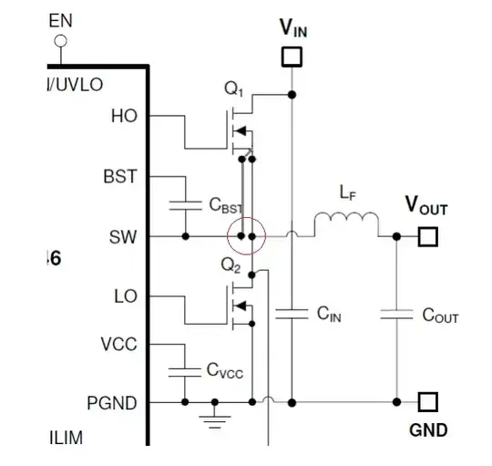
But, in the LM5146-Q1 controller, the voltage from SW pin is also used in the adaptive deadtime delay subcircuit. How disconnecting this pin from external transistor high-current paths may affect switching losses, cannot be predicted without knowing the details of the controller internal circuitry.
LM5146-Q1 might be designed lacking capability to benefit from driving Kelvin-pin-enabled transistors. Having no direct instructions from TI documents, one can only test, measure, and analyze design improvements in order to come up with a better solution (if it is ever possible). Or you can ask the advice of TI engineers on e2e.ti.com forums.


