This is one of those cases where less is better. Let's start out with an old stand-by BJT DC-bias circuit:
simulate this circuit – Schematic created using CircuitLab
The AC loading this presents to the passive phase-shifter is going to be painful (\$r_\pi\$ will dominate everything else about it.) But it has gobs of DC voltage gain to make up for it.
Let's start with a datasheet for an NPN: an OnSemi 2N2222A at MIT's site.
This BJT appears to just beg for a collector current of about \$1\:\text{mA}\$. And you can see that the \$\beta\$ just varies all over the place. We get \$\beta_{_\text{0}}=\sqrt{75\cdot 325}\approx 150\$ and about \$\pm\,50\%\$ variation around that figure.
Hmm, coincidentally, I just happened to use that figure, somewhere. when writing about how to bias one of these things. The number I came up with is that the collector current will vary by about \$\pm\,15\,\%\$ variation given the \$\beta\$ variation I just uncovered in the 2N2222A, above.
So, if we are going to design for \$1\:\text{mA}\$ this means we should expect up to about \$1.2\:\text{mA}\$ (rounding up) as the worst case variation in that direction and as little as about \$800\:\mu\text{A}\$ in the other direction. The design needs to accommodate that fact. It also means that the voltage gain will similarly vary by \$\pm\,15\,\%\$ around whatever we think it might be at \$I_{_\text{C}}=1\:\text{mA}\$.
The voltage gain involves a lot of minor details, like the bulk base impedance reflected to the emitter and the emitter bulk resistance. But these will be under \$1\:\Omega\$. The major detail will be the AC dynamic emitter resistance:
$$r_e^{\:'}= \frac{V_T}{I_{_{\text{E}_\text{Q}}}}$$
And the voltage gain will be:
$$A_v = \frac{R_{_\text{C}}}{r_e^{\:'}}= \frac{R_{_\text{C}}}{\left[\frac{V_T}{I_{_{\text{E}_\text{Q}}}}\right]}=\frac{R_{_\text{C}}}{V_T}\cdot I_{_{\text{E}_\text{Q}}} =\frac{R_{_\text{C}}}{V_T}\cdot\frac{V_{_\text{CC}}-V_{_{\text{C}_\text{Q}}}}{R_{_\text{C}}}\cdot\frac{\beta+1}{\beta}\approx \frac{V_{_\text{CC}}-V_{_{\text{C}_\text{Q}}}}{V_T}$$
Clearly, if we want higher voltage gain then we want to lower the collector voltage. But not too far because we have to accommodate BJT variation mentioned earlier. I'd nominally like to see the collector voltage about \$2\:\text{V}\$ above ground, suggesting a collector resistor close to \$8\:\text{k}\Omega\$. But I need to allow for that margin, so let's use \$R_{_\text{C}}=6.8\:\text{k}\Omega\$, with the idea that nominally \$V_{_\text{C}}=10\:\text{V}-6.8\:\text{k}\Omega\cdot 1\:\text{mA}=3.2\:\text{V}\$. That should be enough margin.
Given \$800\:\mu\text{A}\le I_{_\text{C}}\le 1.2\:\text{mA}\$ then we now find \$1.84\le V_{_\text{C}}\le 4.56\:\text{V}\$. That's quite a lot! (It should almost certainly be \$2.1\le V_{_\text{C}}\le 4.2\:\text{V}\$ using the 15% figure earlier.)
This then also suggests \$210 \le A_v \le 310\$. (The thermal voltage should be about \$26\:\text{mV}\$.) That's without taking any passive loading losses. That's our maximum working value.
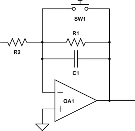
So now we are at the question of losses. But before that, let's look at your two possible 3-resistor + 3-capacitor passive networks (on the right):
simulate this circuit
If we connect the top version to OUT then \$R_1\$ is just a stupid drag on the collector and reduces the signal for no good reason. Instead, if picking that one we should just kill \$R_1\$ and consider \$R_{_\text{C}}\$ as fulfilling that role.
If we connect the bottom version to OUT then \$R_3\$ is going to totally mess up the DC biasing of the BJT. The DC biasing does also represent a resistance, though. So we should just kill \$R_3\$.
Either way, you don't get to keep your pretty little passive section intact unless you bend over backwards like you did in your schematic. Which is also wrong!!
The more sensible thing to do is to remove one of the resistors at either end -- doesn't matter -- and move on. So here's the circuit:
simulate this circuit
The analysis for frequency isn't so easy because \$r_\pi\$ itself will be widely varying. And I'm not going to bother with an attempt because it would at least triple what I've already written. I'll just say that you should keep the values of \$R_2\$ and \$R_3\$ above in the general vicinity of \$R_{_\text{C}}\$.
Finally, \$R_{_\text{B}}\$ should be set pretty high. Just enough to supply the needed base current at the worst case \$\beta\$. In this case, that probably means about \$220\:\text{k}\Omega\$. If this doesn't work for you on the protoboard, make it about twice that and see.
So here's a suggestion for your \$V_{_\text{CC}}=10\:\text{V}\$ case:

simulate this circuit
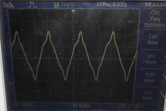
If it doesn't oscillate either select still higher values for the base resistor or else lower the values of \$R_2\$ and \$R_3\$ to load things down a little more there.
Oh. A final note. You specified \$400\:\text{pF}\$ capacitors. If you are using a protoboard you may prefer nanofarads or higher. The boards are notorious for stray capacitance. I can't say that it matters in this case. But it is worth keeping in mind.


